The Intel Core i3-7350K (60W) Review: Almost a Core i7-2600K
by Ian Cutress on February 3, 2017 8:00 AM EST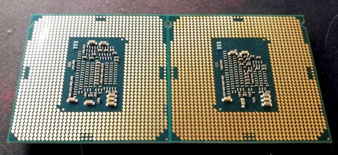
For some intrepid enthusiasts, this is the chip from Intel we’ve been waiting for. I foolishly predicted that Intel would never create an overclockable Core i3, because it had the potential to drive sales away from high-margin products. But here we are, Core i3-7350K in hand, and the ability to drive almost 5.0 GHz without too much trouble. This raises a couple of questions: just how close is it to the cheapest Core i5-7400 out of the box, which is only a few dollars more, and how close is it to the Core i7-2600K, a favorite chip among enthusiasts who have not yet upgraded.
Slap Me On The Wrist
For the previous generation of Intel products, we reviewed the Core i3-6100TE. This was a low-powered Core i3, but it was paired with the SuperMicro C7H170-M, a motherboard that enabled adjustment of the base frequency from 100 MHz to 130 MHz and up. This was the first chance in a number of generations to test what would essentially be an overclockable Core i3 product. There were many teething issues, as overclocking via the base frequency is less stable than by the multiplier, plus the motherboard options were not the easiest to work with.
![]()
However the final conclusion was that the Core i3 parts, while having two cores and hyperthreading, have difficulty keeping up with the Core i5 in tasks where having actual cores matter. For gaming, especially 1080p or Full-HD gaming, there was a small difference in favor of the Core i5, and the indication that with DX12 enabling multi-core gaming in a nicer way before, a gap would likely emerge over time (but mainly for high-end games for now). As a result, we postulated that Intel would never release a Core i3-K product: doing so would potentially drive sales away from the i5-K, as here is a part that could perform just as well for $60-$70 less, which users would have in pocket to upgrade a graphics card instead.
Can Die Size Account for the Difference?
Intel, from the outside, seems very margin driven: keeping those numbers above 60-65% in every department seems to be key to progress. As a result certain projects come and go, and others with potential have a small grace period but the bottom line is performance and strategy. One could argue that potentially offering an easy route for users to migrate down from a Core i5-K to a Core i3-K could affect that bottom line: users are paying $60 less per unit, and that’s a $60 loss per sale. This is one way of looking at it – another is considering that the Core i3-K parts are dual-core by design, and cheaper to make.
Disclaimer: The data for 2+2/4+2 Kaby Lake and Skylake for the following analysis were derived from high quality images of each die, and thus subject to error.
| CPU Die Size Comparison Numbers in table are to nearest degree of known accuracy Data from Intel or Trusted Sources (Chipworks/PCWatch) |
||||||
| CPU | Year | Process Node |
Die Size 2C or 2+2 |
Die Size 4C or 4+2 |
Die Size 4+3/e (no eDRAM) |
Die Size (other) |
| Intel Kaby Lake | 2017 | 14+nm | 98.68 | 126.15 | - | |
| Intel Skylake | 2015 | 14nm | 98.57 | 122.40 | 234 | - |
| Intel Broadwell | 2014 | 14nm | 82 | *** | 241.50 | 133 (2+3) 246.24 (10C) 306.18 (15C) 456.12 (24C) |
| Intel Haswell | 2013 | 22nm | 130 | 177 | 264 | 181 (2+3) 355.52 (8C) 492 (12C) 662 (18C) |
| Intel Ivy Bridge | 2012 | 22nm | 118.09 | 159.82 | - | 256.5 (6C) 341 (10C) 541 (15C) |
| Intel Sandy Bridge | 2011 | 32nm | 149 | 216 | - | 435 (8C) |
| Intel Westmere (GPU on 45nm) |
2009 | 32nm | 81 (Core) 195* (+GPU) |
276** | - | 248 (6C) 513 (10C) |
| Intel Nehalem | 2008 | 45nm | - | 263 | - | 296 (HEDT) 684 (8C) |
| Intel Yorkfield | 2007 | 45nm | 107 | 220 | - | - |
| Intel Kentsfield | 2007 | 65nm | - | 280 | - | - |
| Intel Conroe | 2006 | 65nm | 145 | - | - | - |
Italicised numbers are calculated from images and represent more of a 'peak' die size. Data taken from delidded images varied wildly, from 105mm2 to 130mm2 for the 4+2, so should be taken under caution.
* Dual Core Westmere CPUs had a IGP built on 45nm
** Quad Core Westmere designs with IGP didn't exist, so this is an estimate of what it would have been
*** Broadwell 4+2 designs don't seem to exist. The two mobile parts (we don't have access to) that fit this description are likely to be cut down 4+3e parts.
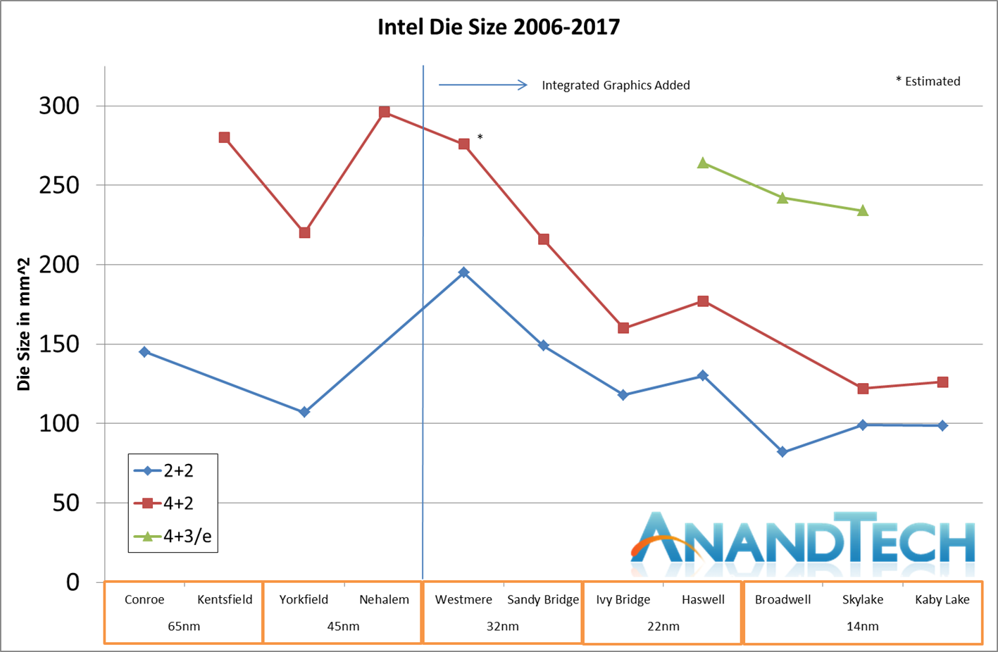
Taking data from available images on delidding the dual core parts and quad core parts, it’s clear that the new generation of Kaby Lake processors are physically smaller than Skylake. But the difference between the Core i5/i7 core design (known as 4+2) and the Core i3 design (known as 2+2) isn’t that much. With a die size of 126.15 mm2 for the quad core and 98.68 mm2 for the dual core, the die sizes of the two chips are relatively close, with a difference of just 27.47 mm2. This makes the dual core design 78% of the quad core size. If costs scaled linearly with die size, then die size difference between the two (22%) equates to $52.75 of the cost of the i5-7600K list price. This is similar to the list price difference between the two chips as a whole.
As we have this data for the first time, it is interesting to see that Intel’s new method of ‘Process-Architecture-Optimization’ rather than Tick-Tock, is yielding results. The Skylake 4+2 die size is similar from 122 mm2 to 126 mm2, and goes in line with the fact that Intel has officially stated that one of the key features of the new 14+ process is that the transistors are more ‘relaxed’ and there’s no decrease in density. Exactly what that means is likely under wraps for all but Intel (or Chipworks). But the difference between Kaby Lake 4+2 and 2+2 also means that we can get a rough number for the die area required for two cores.
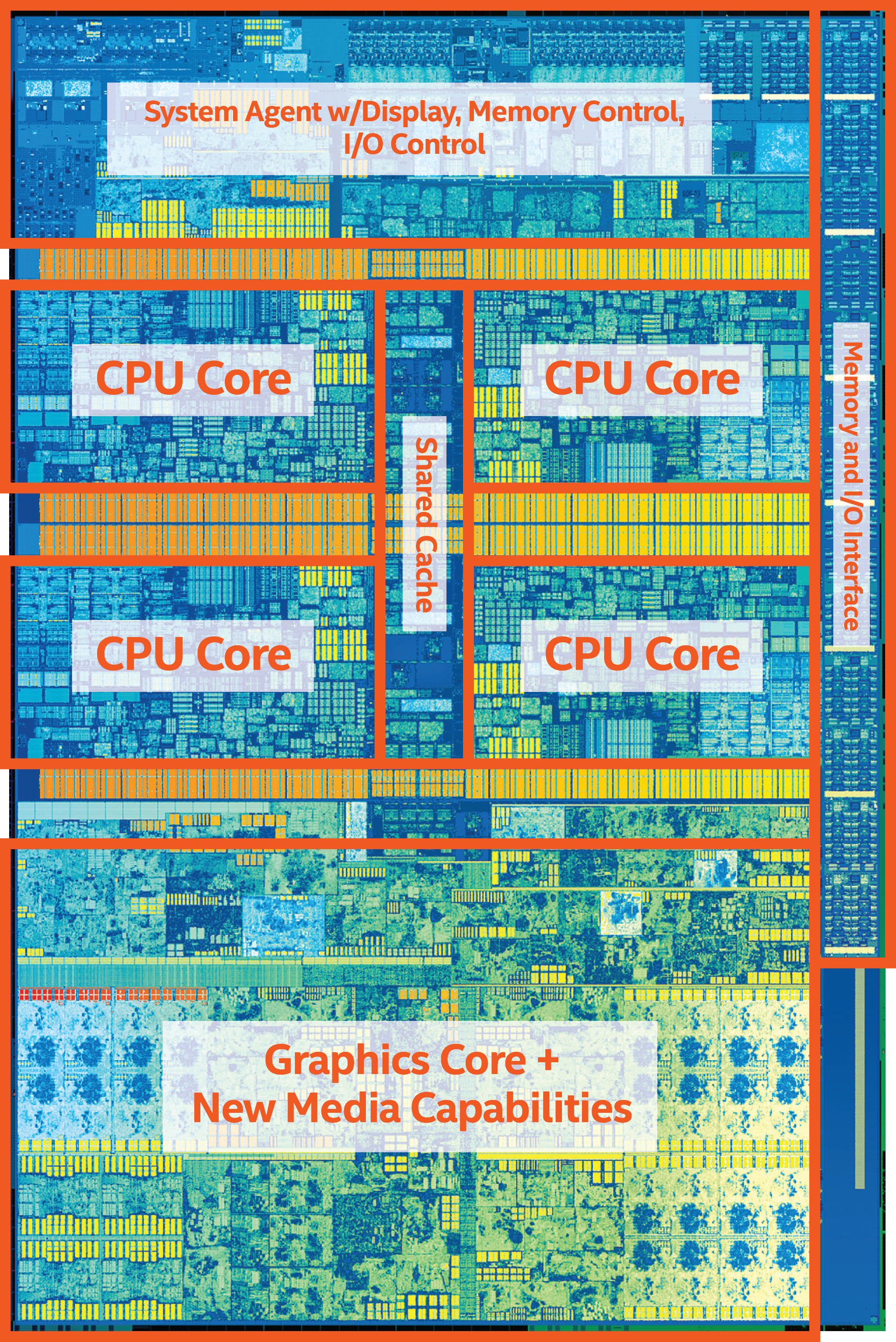
In this case, two Kaby Lake cores plus L3 cache (plus periphery required for another two cores) are approximately 27.47 mm2. This makes the two cores in the dual core design approximately (given sufficient error margin) 27.8 % of the die. Doubling the die size for the four core version means that the CPU cores take up ~43% of the design. It's worth noting that using Intel's official die shot of the quad-core above puts the core area at around the 33-37% mark, depending on how you count the interconnect. The GPU area is almost identical (within 1%) of the core area as well. Our numbers here are calculated from delidded CPUs rather than official numbers, as Intel sporadically gives out such numbers these days (it depends which department is making the announcement, oddly) which makes our results more of an upper limit which is important to consider.
Because of the image above, we could arguably call the GT2 graphics inside the quad core design equal in size to the CPU cores (which seems plausable) at 54.94 mm2, then using the full dize size measurement above, it leaves 16.27 mm2 for the memory controller, system agent, and other requirements. If we do the math back into the dual core design with the same graphics core, we get 16.27 mm2 for the memory controller and other requirements as well.
| Kaby Lake Comparison | |||||
| CPU | Die Size | Cores | Core Area | GT2 Area | IMC + other |
| Intel Kaby Lake-S 4+2 | 126.15 | 4 | 54.94 | 54.94 | 16.27 |
| Intel Kaby Lake-S 2+2 | 98.68 | 2 | 27.47 | 54.94 | 16.27 |
For clarity, numbers in bold are measured; italics are estimates, and others are calculated.
So if the difference in die size can account for the price difference and won’t affect margins, what’s the bottom line here? Ultimately $60-70 per sale lost is a drop in revenue. However, it also depends on yields, and how the different CPUs are being binned. That information we won’t ever have. What we do know is that the Core i3-7350K is coming onto shelves at the end of January/beginning of February, rather than with the rest of the Kaby Lake CPUs in early January. So perhaps, ultimately, the effect of offering a Core i3-K in this case is minimal to Intel’s bottom line.
But Where Does the Core i3-7350K Fit In?
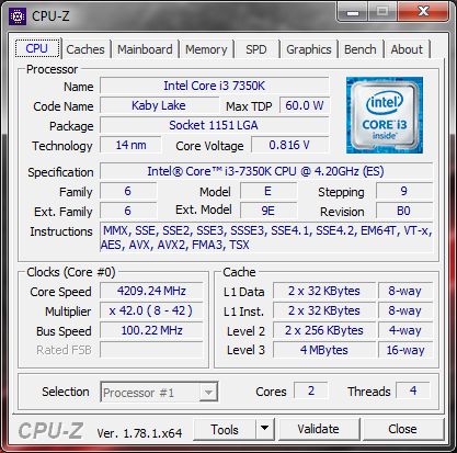
Intel's 7th Generation of Core CPUs, which often goes by its internal code name 'Kaby Lake', stretches from 91W on the mainstream desktop down to 4.5W for notebook processors, all using the same underlying technology in different core and integrated graphics configurations. The i7-7700K is the top part of this processor family, featuring four cores with hyperthreading, and we move down through the Core i5 and Core i3 parts. This time there are three overclocking processors, with the new one being the Core i3-7350K.
| Intel Kaby Lake S SKUs | |||||||
| Cores/ Threads |
Base/ Turbo |
IGP | L3 | eDRAM | TDP | Cost OEM |
|
| i7-7700K | 4/8 | 4.2/4.5 | HD 630 | 8 MB | - | 91 W | $339 |
| i7-7700 | 4/8 | 3.6/4.2 | HD 630 | 8 MB | - | 65 W | $303 |
| i7-7700T | 4/8 | 2.9/3.8 | HD 630 | 8 MB | - | 35 W | $303 |
| i5-7600K | 4/4 | 3.8/4.2 | HD 630 | 6 MB | - | 91 W | $242 |
| i5-7600 | 4/4 | 3.5/4.1 | HD 630 | 6 MB | - | 65 W | $213 |
| i5-7600T | 4/4 | 2.8/3.7 | HD 630 | 6 MB | - | 35 W | $213 |
| i5-7500 | 4/4 | 3.4/3.8 | HD 630 | 6 MB | - | 65 W | $192 |
| i5-7500T | 4/4 | 2.7/3.3 | HD 630 | 6 MB | - | 35 W | $192 |
| i5-7400 | 4/4 | 3.0/3.5 | HD 630 | 6 MB | - | 65 W | $182 |
| i5-7400T | 4/4 | 2.4/3.0 | HD 630 | 6 MB | - | 35 W | $182 |
| i3-7350K | 2/4 | 4.2 | HD 630 | 4 MB | - | 60 W | $168 |
| i3-7320 | 2/4 | 4.1 | HD 630 | 4 MB | - | 51 W | $149 |
| i3-7300 | 2/4 | 4.0 | HD 630 | 4 MB | - | 51 W | $138 |
| i3-7300T | 2/4 | 3.5 | HD 630 | 4 MB | - | 35 W | $138 |
| i3-7100 | 2/4 | 3.9 | HD 630 | 3 MB | - | 51 W | $117 |
| i3-7100T | 2/4 | 3.4 | HD 630 | 3 MB | - | 35 W | $117 |
| G4620 | 2/4 | 3.7 | HD 630 | 3 MB | - | 51 W | $86 |
| G4600 | 2/4 | 3.6 | HD 630 | 3 MB | - | 51 W | $75 |
| G4600T | 2/4 | 3.0 | HD 630 | 3 MB | - | 35 W | $75 |
| G4560 | 2/4 | 3.5 | HD 610 | 3 MB | - | 54 W | $64 |
| G4560T | 2/4 | 2.9 | HD 610 | 3 MB | - | 35 W | $64 |
| G3950 | 2/2 | 3.0 | HD 610 | 2 MB | - | 51 W | $52 |
| G3930 | 2/2 | 2.9 | HD 610 | 2 MB | - | 51 W | $42 |
| G3930T | 2/2 | 2.7 | HD 610 | 2 MB | - | 35 W | $42 |
The Core i3-7350K is the odd member of the stack. It sits as the only processor with a TDP of 60W, and is priced very close to the Core i5-7400/7400T. The comparison between this two (we were able to run limited tests on the i5-7400) will be a key aspect to this review given the pricing – will an extra $14 for two more cores offset the fact that the Core i3-7350K has a super high base frequency? Having 4.20 GHz as the frequency of the Core i3-7350K is interesting: as a Core i3, it has no turbo mode per-se, and it operates either in a low power mode (800 MHz or so) when idle or at full throttle when needed. This has some advantages over a turbo mode by having peak power being the only consideration, especially when combined with Windows 10 and using Intel’s Speed Shift technology to ramp up to the top speed quickly.
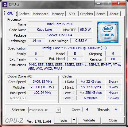
Intel Core i3-7350K vs Core i5-7400
Aside from the physical cores, the Core i3-7350K has less cache than the Core i5-7400, which is something to note.
One other pertinent comparison I want to make in this review is with the perennial favorite of DIY system builders for the last seven years or so: the Core i7-2600K. This is the high-end processor from the Sandy Bridge family that is known for being a good overclocker and a part which a lot of users are still on due to the lack of distinct performance improvements over the recent Intel microarchitectures. For most users still on these parts, the upgrade to a newer platform does not offer a substantial enough performance uptick to validate the outlay. However, at one point, there is going to be a Core i3 performance CPU that matches the Core i7-2600K. I want to find out if that time is now, or how far it might be away.
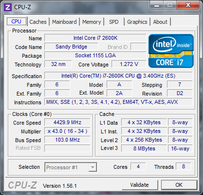
Intel Core i3-7350K vs Core i7-2600K (overclocked)
| Kaby Lake i3 vs Sandy Bridge i7 Comparison Launch Pricing |
|||||||||
| CPU | Year | Cores Threads |
Freq | Turbo | L3 | IGP | DRAM | TDP | Price |
| Core i3-7350K | 2017 | 2/4 | 4.2 | - | 4MB | HD 630 | DDR4-2400 | 60W | $168 |
| Core i7-2600K | 2011 | 4/8 | 3.4 | 3.8 | 8MB | HD 3000 | DDR3-1333 | 95W | $317 |
In simple numbers, the Core i7-2600K has a base frequency of 3.40 GHz and has a turbo up to 3.8 GHz. The Core i3-7350K is at 4.2 GHz, giving it both a frequency advantage and 35%+ advantage in instructions per clock (IPC) by virtue of being so many generations ahead. Aside from the L3 cache difference, and the move from DDR3 to DDR4, is there a sufficient frequency and IPC increase for the Core i3 to match the golden processor of yesteryear? This review will solve that question.
More about Kaby Lake
For readers that want a more in-depth take on Kaby Lake as a platform, we have a dedicated article full of information for you. We also have other articles in our Kaby Lake bonanza.
Other articles include:
Intel Launches 7th Generation Kaby Lake (Overview and Core Improvements)
The Intel Core i7-7700K Review: The New Out-of-the-box Performance Champion
The Intel Core i5-7600K Review: The More Amenable Mainstream Performer
The Intel Core i3-7350K Review: When a Core i3 Nearly Matches the Core i7-2600K (This Review)
Still to come
Calculating Generational IPC Changes from Sandy Bridge to Kaby Lake
Intel Core i7-7700K, i5-7600K and i3-7350K Overclocking: Hitting 5.0 GHz on AIR
Intel Launches 200-Series Chipset Breakdown: Z270, H270, B250, Q250, C232
Intel Z270 Motherboard Preview: A Quick Look at 80+ Motherboards


186 Comments
View All Comments
Bullwinkle J Moose - Sunday, February 5, 2017 - link
Correction: Can I record what I hear on the desktop with the DRM crippling API's found in Windows Vista / 7 / 8 and 10 ?should be > Can I record what I hear on the desktop with the DRM "crippled" API's found in Windows Vista / 7 / 8 and 10 ?
The API's do not cripple the DRM
The DRM does all the crippling !
Bullwinkle J Moose - Sunday, February 5, 2017 - link
Finally got Optical SPDIF working in both Windows 8.1 AND Windows 10 after that rant above!Yes, I Really did think that was a DRM issue
My original USB Soundblaster had optical in and out disabled in software updates after all the hysterical copyright violation complaints
Meteor2 - Sunday, February 5, 2017 - link
RE: why are there no 150-200W consumer CPUs. Because there's no consumer software which could take advantage of 24C/48T CPUs, unlike GPUs.Of course, if you want a 150W CPU, you can buy a big Xeon. But there's not a lot of software out there which can make use of them.
The_Assimilator - Monday, February 6, 2017 - link
Should've rather used an i5-2500K in the comparison; 2c/4t vs 4c/4t is fairer than 4c/8t. Although, a real comparison at 4.6GHz on both chips (or whatever the i3 can hit) would see the KBL obliterated regardless.evilpaul666 - Wednesday, February 8, 2017 - link
I think they said they're working on an overclocking article, but I agree the i5-2500K with both chips overclocked would have been a much more interesting test.Anato - Monday, February 6, 2017 - link
Intel should make all K-processors fully enabled, HT, ECC, Cache and sell them cheaply as 2.0-3GHz parts. Then give user tools to make changes to cache, ECC etc and after that its users task to find out what CPU can do. That would bring back good old days and Intel could get rid of cores that are otherwise unsellable.Still no need to upgrade from Sandy Bridge i5-2500k and just bought GTX 1080 for it.
evilpaul666 - Wednesday, February 8, 2017 - link
So is Optane ever actually coming out? And is it going to actually work as a 16/32GB cache for mechanical storage the ~1500/500 read/write speeds I saw quoted for it a while back would be nice as a cache for HDDs, but are slower than NVMe drives at this point.evilspoons - Wednesday, February 8, 2017 - link
Well, I guess I'm *still* sitting on my i7-2600k overclocked to 4.6 GHz. I pushed it from stock clocks in ~2013 assuming I'd replace it soon but four years later it's still ticking along just fine and I still don't have a compelling upgrade path!ANobody - Wednesday, February 8, 2017 - link
Slow is the death of IPC progress. Painful to watch.Ubercake - Friday, February 10, 2017 - link
I would hope an i3 marketed as 5 generations later could match an i7 from 5 generations before?Intel has had the market cornered for too long...