Infineon Shows Off Future of eSIM Cards: <1.65 mm2 Made Using 40 nm
by Anton Shilov on March 11, 2017 5:00 PM EST- Posted in
- MWC_2017
- Mobile
- Trade Shows
- Smartwatch
- eSIM
- Infineon
- M2M
- SIM
Update 3/20: Infineon has contacted us and said that the eSIM IC is made using a 40 nm process technology.
At MWC this year, Infineon showcased a lineup of its current and embedded SIM products. The company demonstrates not only the industry-standard MFF2 eSIM chip, but also considerably smaller ICs designed for future miniature devices (many of which may not even exist yet as a category) as well as M2M (machine to machine) applications. It is noteworthy that to manufacture an eSIM the size of a match head, Infineon uses GlobalFoundries 14LPP a 40 nm process technology, taking advantage of leading-edge lithography to bring the size of a simple device down.
The first SIM cards were introduced in 1991 along with the world’s first GSM network operated by Radiolinja in Finland (now the company is called Elisa). Back then, mobile phones were so bulky that a card the size of a credit card (1FF) could fit in. Eventually, handsets got smaller, Mini-SIMs (2FF) replaced full-sized SIMs and then Micro-SIM (3FF) and Nano-SIM (4FF) cards took over. While mobile phones have evolved considerably in terms of feature-set in the last 25 years, the function of the SIM card remained the same: it stores an integrated circuit card identifier (ICCID), an international mobile subscriber identity (IMSI), a location area identity, an authentication key (Ki, this part actually requires a basic 16- or 32-bit compute unit) as well as a phone book and some SMS messages.
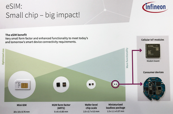
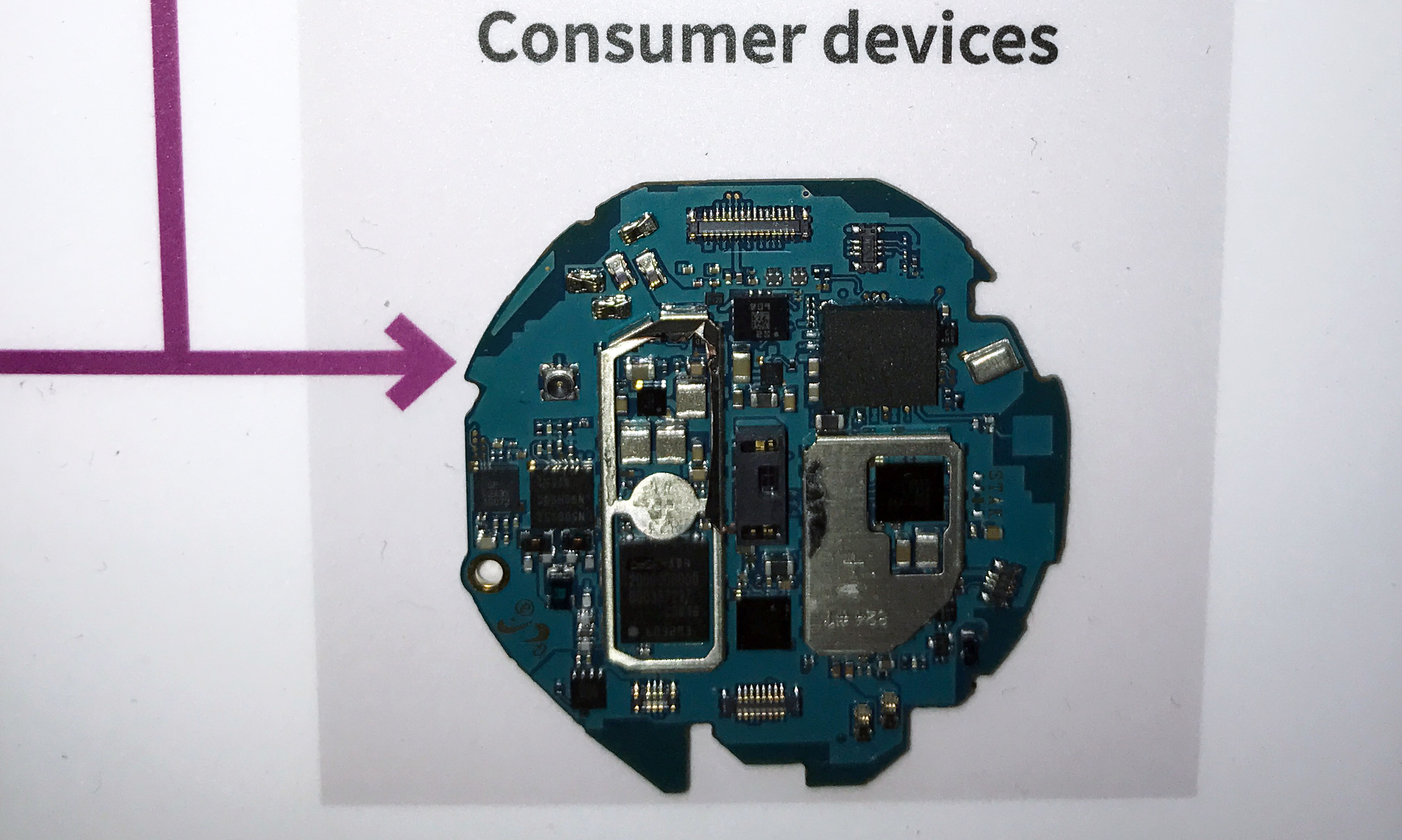
By today’s standards, the amount of data that each SIM card stores is so tiny that its physical dimensions are simply not justified. Even Nano-SIMs are too large for applications like a smartwatch, and this is when embedded SIMs come into play: their form-factor is considerably smaller, they can be used with various operators (which makes them more flexible in general) and some of such cards have an expanded feature set (e.g., hardware crypto-processors). Today, there is one internationally recognized form-factor for eSIMs, the MFF2, which is used inside devices like Samsung’s Gear series smartwatch with GSM/3G connectivity. If we actually take a look inside the Gear S2 smartwatch, we will notice that the eSIM is actually one of the largest components and its functionality is disproportional to its dimensions.
At MWC 2017 Infineon is demonstrating two more eSIM implementations, which have not been standardized (yet?), but which are already used inside millions of devices.
The first one, when packaged, has dimensions of 2.5×2.7×0.5 mm, which essentially means that it has no packaging at all. This IC is produced using a mature 65 nm process technology and that means that it is very cheap.
The second eSIM implementation that Infineon demonstrates is actually even tinier: its dimensions when fully packaged and ready to use are just 1.5×1.1×0.37 mm. The IC is made using a 40 nm process technology. Using an advanced process technology to make eSIM cards is not something common, but the approach enables developers of various devices to take advantage of the smallest cards possible (another advantage of such cards are low voltages and power consumption).
It remains to be seen when the industry formally adopts eSIM standards smaller than the MFF2, but dimensions of the eSIMs that Infineon is demonstrating clearly indicate that there are ways to make these cards smaller. Moreover, companies are not afraid of using proprietary/non-standard form-factors are already using the offerings from Infineon. It is up for debate whether using leading-edge process technology for making eSIMs makes sense in general (after all, far not all devices require tiny dimensions and expanded functionality of eSIMs, such as crypto-processors), but with 10 million non-standard eSIMs shipped to date it is obvious that there are mass market devices that can absorb such chips even at potentially premium pricing.
Source: Infineon


28 Comments
View All Comments
Valantar - Monday, March 13, 2017 - link
How are you supposed to log in to anything if you're not even connected to a network? Who is going to host and maintain this login service? How will handoffs happen if the network recieving your "login" isn't the one you're a subscriber to? If you open up the networks to "unauthorized" use, to allow for logins like this, how do you avoid this being abused for other means? How do you avoid account theft and/or spoofing? Neither of these are trivial questions.name99 - Monday, March 13, 2017 - link
You are right that these are not trivial questions. You are wrong in assuming that they don't have answers. Consider two different types of technologies- Apple Pay
- the programmable SIM built into cellular iPad Air 2
(I am most familiar with Apple technologies; other vendors doubtless have similar technologies)
Point is, these are two technologies that address your points and exist today. They could be extended to a complete solution. What's preventing this today is 100% the carriers' desire to maintain control over their users, nothing to do with technology.
piroroadkill - Sunday, March 12, 2017 - link
I don't want smaller SIMs. I like human-usable SIMs. The nano-SIM is small enough.Gunbuster - Sunday, March 12, 2017 - link
SIM functionality should have been rolled into MicroSD long ago. Streamline to one slot and no more bitching about storage. Oh but then how would they upsell to $1100 phones...haukionkannel - Monday, March 13, 2017 - link
Easily... just make the basic model 1200$ and then give 10% super discount...Valantar - Monday, March 13, 2017 - link
Eh ... so if your SD card was too small or failed (which is quite common), you would need to activate your new SD card with your carrier, and be without phone service if the card failed? Yeah, that's a great idea.TheinsanegamerN - Monday, March 13, 2017 - link
Well, lets see. Any time I need more storage, or the SD card fails (which is comon) I would need to go buy and activate a new SIM card, all the while having no cell contact, to save half a fingernail's worth of space.yeah. great idea.
How about making the phone 1 mm thicker instead.
Valantar - Monday, March 13, 2017 - link
Am I the only one wondering how on earth you implement an IC that small with some form of meaningful interface to the board? How can that fit more than 2-3 solder pads at the most? I mean, 1.5x1.1mm is .. a third of a grain of rice? One thing is miniscule surface mount capacitors and resistors, which have two distinct ends and no need of more complicated connections than that. Another thing entirely is a data storage unit with R/W capability. I'm not saying it's impossible, I just can't figure out how it would work. Then again, I'm not an engineer of any kind.