Samsung’s 8LPP Process Technology Qualified, Ready for Production
by Anton Shilov on October 19, 2017 11:00 AM EST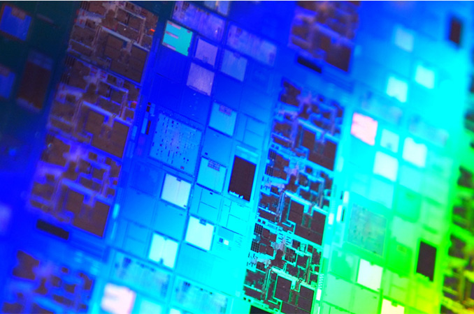
Samsung this week announced that its 8LPP fabrication process, which it formally introduced earlier this year, had passed qualification tests. The manufacturing technology will be used to produce advanced SoCs next year and will be Samsung’s final leading edge process based solely on DUV lithography before the company adopts EUV for select layers with its 7LPP process node.
The 8LPP fabrication technology is an evolution of Samsung’s 10 nm node that uses narrower metal pitches and promises a 10% area reduction (at the same complexity) as well as a 10% lower power consumption (at the same frequency and complexity) compared to the 10LPP process. Samsung does not disclose which standard cell libraries are used by the 8LPP, but the 10LPP relies on 8.75T and 10.5T, so it is logical to expect the 8LPP to use similar ones. Samsung does not disclose whether the 8LPP relies on quadruple patterning techniques, or if it continues to use triple patterning like the company’s 10LPE/10LPP processes, but QPT is an option to shrink die sizes at the increase in cost (and potential defects).
| Advertised PPA Improvements of New Process Technologies Data announced by companies during conference calls, press briefings and in press releases |
||||||||
| 14LPP vs 28LPP |
10LPE vs 14LPE |
10LPE vs 14LPP |
10LPP vs 10LPE |
10LPU vs 10LPE |
8LPP vs 10LPP |
|||
| Power | 60% | 40% | 30% | ~15% | ? | 10% | ||
| Performance | 40% | 27% | >10% | ~10% | ? | ? | ||
| Area Reduction | 50% | 30% | 30% | none | ? | 10% | ||
Samsung plans to use the 8LPP manufacturing technology to produce SoCs for various applications, including smartphones, cryptocurrency and networks/servers, but does not elaborate on exact designs or clients. The only thing we do know is that Qualcomm will be one of the first customers to adopt the 8LPP and that the company expects the new technology to ramp up fast (which possibly means that it uses the same libraries and manufacturing equipment as the 10 nm nodes).
“8LPP will have a fast ramp since it uses proven 10 nm process technology while providing better performance and scalability than current 10nm-based products” said RK Chunduru, a senior vice president of Qualcomm.
Neither Samsung nor Qualcomm are disclosing when they expect to ship their first 8LPP chips, but since the technology has passed qualification tests (meaning that quality and reliability of ICs made using the technology meet certain guidelines, such as those proposed by JEDEC), we would expect the SoCs to arrive in the coming quarters.
Related Reading
Source: Samsung


34 Comments
View All Comments
HStewart - Thursday, October 19, 2017 - link
Please look at the following Article from Amandtechhttps://www.anandtech.com/show/11928/intels-docume...
This is for Ice Lake - and if Intel does a significant speed up - it will be a game changer.
Wilco1 - Friday, October 20, 2017 - link
Yes I've read the article and nothing in it indicates there will be a major speedup. All we know is Ice Lake will reduce the micro code penalty. Given REP MOV is practically never used precisely because it is so slow, it can't give a major speedup in existing code.HStewart - Friday, October 20, 2017 - link
"Given REP MOV is practically never used precisely because it is so slow, it can't give a major speedup in existing code."Question have you ever program in assembly or look at code that compiler generates - especially with string moves - in my experience REP MOV is used a lot and all over the place - but yes it is older x86 instruction then some of newer extensions like AVX-512. But keep in mind there is a lot of versions of REP MOV based on size of operand.
But it appears Intel is aware of the slowness and importance of this instruction
https://software.intel.com/en-us/forums/intel-visu...
Keep in mind I have not used Intel assembly programing for about 25 years and a lot of advancements have happen since. But I am still knowledgeable about CPU design but not as much when I was doing OS development. Just the need for ASM developers is pretty much gone away. In fact back 1992, I did interview with Intel and they actually did not need ASM developers.
name99 - Friday, October 20, 2017 - link
Why is "how many transistors can be pack[ed] in [the] same area" an important metric?Sure that might matter if you want you want to produce is a slab of SRAM, but most people demand more than that from their SoCs...
I obviously have no idea exactly what will be in, say, Canon Lake or Ice Lake, but if Intel is covering their SoCs just with SRAM caches because they can't think of anything more to add, while Apple (and others like Huawei) are adding LOGIC rather than caches (so ever more sophisticated GPUs, ISPs, and now NPUs) then it's not really of much interest to say that Intel has higher transistor density. Yeah, so what? All that's telling us is that Intel is putting vastly more "easy" transistors on their chips while the competition is putting many more "hard"(ie much more varied, much more random wiring) transistors on their chips.
Dr. Swag - Thursday, October 19, 2017 - link
Depends on how you compare it. If you compare Samsung 14nm LPP to Intel Intel definitely is better. If you're talking about 10nm I'm really not too sure, and if it's their 8nm vs. Intel 14nm if I had to guess I'd say Samsung is better.Santoval - Thursday, October 19, 2017 - link
Define "superior". If you mean "transistor density" Intel has clearly the best at every respective xxnm node, which is why they proposed to switch to transistor density in order to compare processes, rather than quote useless xxnm numbers. Transistor density (of the FEOL stack) is simple, clear, unambiguous and independently verifiable, so the company with the highest one can rise on top.So why do you think the other companies avoid it like a plague? I am sure you can hazard a guess.
Wilco1 - Thursday, October 19, 2017 - link
Avoid it? The CPP/MMP/track/SRAM details have all been published. See https://www.semiwiki.com/forum/content/6713-14nm-1...Santoval - Thursday, October 19, 2017 - link
p.s. Not simply transistor density but "transistor density per mm^2", in order to normalize smaller and larger dies.Wilco1 - Friday, October 20, 2017 - link
Here is a slide by Intel comparing transistor density of several Apple chips with Broadwell and Skylake. The part on the left is the real transistor density (so literally #transistors / die size), the part on the right is mostly marketing.http://cdn.wccftech.com/wp-content/uploads/2016/09...
name99 - Friday, October 20, 2017 - link
Umm, do you know what the word density means?I don't want to mock you bcs English may not be your first language, but
"transistor density" means "transistors per mm^2".
There is no such thing as "transistor density per mm^2".