Intel to Create new 8th Generation CPUs with AMD Radeon Graphics with HBM2 using EMIB
by Ian Cutress on November 6, 2017 9:43 AM EST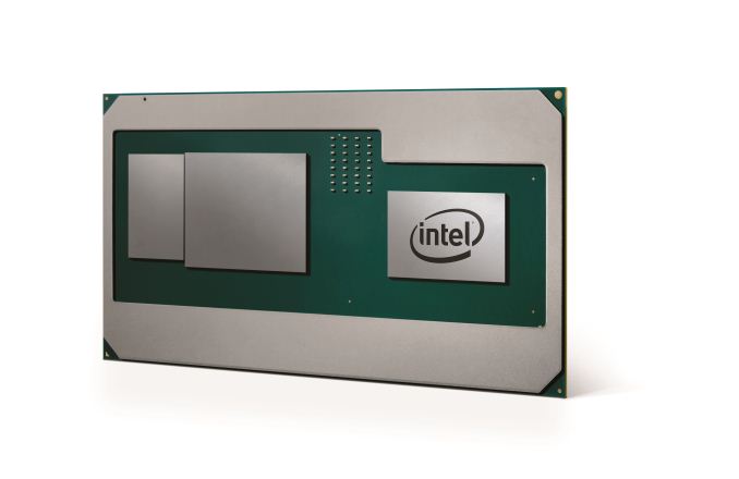
Today we have an announcement out of left field. Intel has formally revealed it has been working on a new series of processors that combine its high-performance x86 cores with AMD Radeon Graphics into the same processor package using Intel’s own EMIB multi-die technology. If that wasn’t enough, Intel also announced that it is bundling the design with the latest high-bandwidth memory, HBM2.
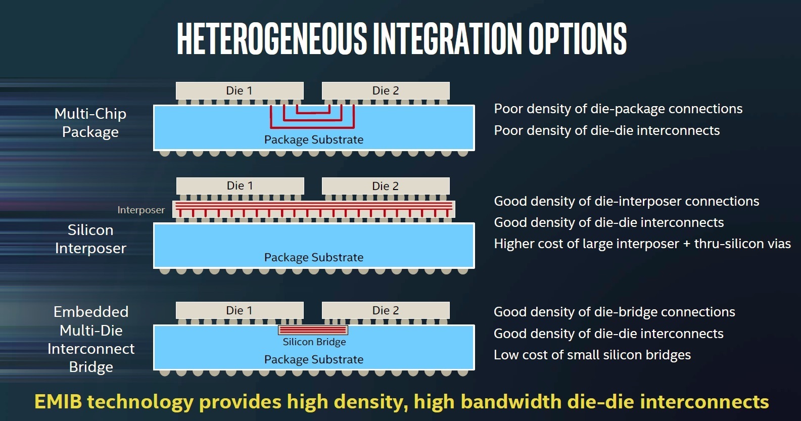
Intel announced its EMIB technology over the last twelve months, with the core theme being the ability to put multiple and different silicon dies onto the same package at a much higher bandwidth than a standard multi-chip package but at a much lower cost than using a silicon interposer. At Intel’s Manufacturing Day earlier this year, they even produced a slide (above) showcasing what might be possible: a processor package with the x86 cores made on one technology, the graphics made in another, perhaps different IO and memory or wireless technologies too. With EMIB, processor design can become a large game of Lego.
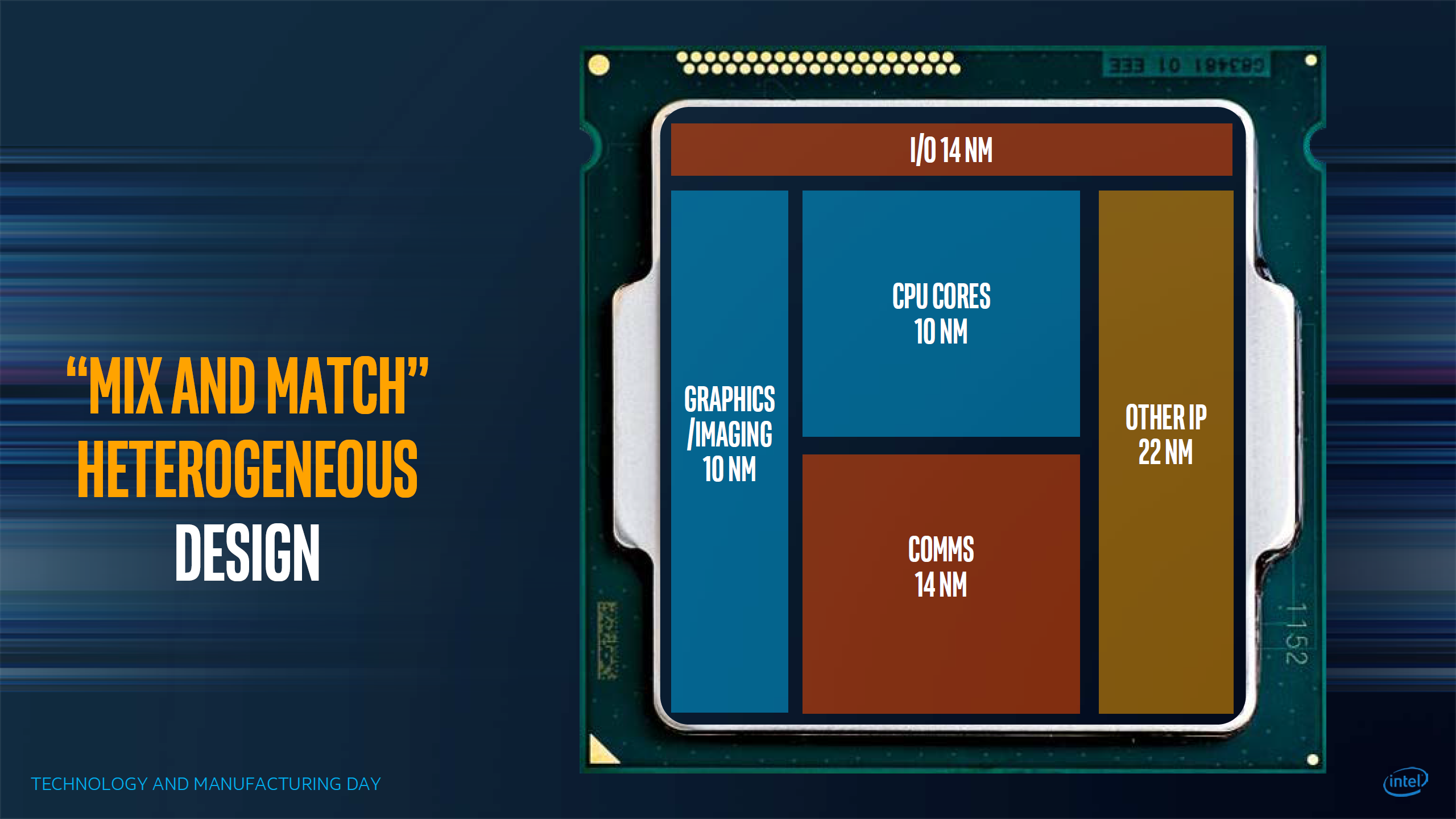

EMIB came to market with the latest Intel Altera FPGAs. By embedding the EMIB required silicon design into the main FPGA and each of the chipsets, the goal was to add multiple memory blocks as well as data transfer blocks in a mix and match scenario, allowing large customers to have the design tailored to what they require. The benefits of EMIB were clear, without the drawbacks of standard MCP design or the cost of interposers: it would also allow a design to go beyond the monolithic reticle limit of standard lithography processes. It was always expected that EMIB would have to find its way into the general processor market, as we start to see high-end server offerings approaching 900 mm2 over multiple silicon dies in a single package.
Since the EMIB announcements, Intel’s Manufacturing Day, and Hot Chips, word has been circulating about how Intel is going to approach this from a consumer standpoint. As part of the requirements of Intel’s own integrated graphics solutions, a 2011 cross-licensing deal with NVIDIA was in place – this deal was set to expire from April 1st 2017, and no mention of extending that deal was ever made public. A couple of rumors floated around that Intel were set to make a deal with AMD instead, as despite their x86 rivalry they were a preferred partner in these matters. Numerous outlets with connections in both AMD and Intel had difficulty prizing any information out. Historically Intel refuses to comment on such matters in advance. Other potential leaks include published benchmarks over at SiSoft, although nothing has been made concrete until today.
Intel’s official statements on the announcement offer a few details worth diving into.
The new product, which will be part of our 8th Gen Intel Core family, brings together our high-performing Intel Core H-series processor, second generation High Bandwidth Memory (HBM2) and a custom-to-Intel third-party discrete graphics chip from AMD’s Radeon Technologies Group* – all in a single processor package.
Intel interestingly uses a singular word for ‘product’, although this does not indicate if it is a family or literally a single SKU in the works. On Intel’s Core-H series processors, these are currently Kaby Lake based running at 45W, with Intel’s integrated GT2 graphics. It would be interesting to see if the graphics of the Core-H are then stripped out as a new silicon design, or if they are re-spinning the full Core-H silicon as a result and just displaying the integrated cores, or are able to run both graphics segments independently (it is likely a new spin of silicon, if I were a betting man). The use of HBM2 is not unsuprirising – Intel has successfully integrated HBM2 into its Altera EMIB-based products so we would suspect that this is not going to be overly difficult.
The next bit is the interesting one: ‘custom-to-Intel … discrete graphics chip’ from AMD RTG. This means that none of AMD’s current product stack has silicon dedicated to EMIB, but AMD is going to leverage its semi-custom design to provide graphics chiplets for Intel to add to its silicon.
‘In close collaboration, we designed a new semi-custom graphics chip, which means this is also a great example of how we can compete and work together, ultimately delivering innovation that is good for consumers… Similarly, the power sharing framework is a new connection tailor-made by Intel among the processor, discrete graphics chip and dedicated graphics memory. We’ve added unique software drivers and interfaces to this semi-custom discrete GPU that coordinate information among all three elements of the platform.’
One of the questions about running multiple chips in a single package is how to manage all the bandwidth and power. AMD has recently solved that issue in its server processors and inside its APUs by using their Infinity Fabric, which if I were to guess would not be under the purview of this collaboration. It states that with collaboration that the chip shares a power framework, which will be an interesting deep dive when we get information as to whether Intel offering separate power rails for the CPU and GPU segments, using an integrated voltage regulator (like Broadwell did), or doing something similar to AMD by using a unified power rail sharing mechanism with digital LDOs as was announced with Ryzen Mobile only a couple of weeks ago.
‘Look for more to come in the first quarter of 2018, including systems from major OEMs based on this exciting new technology.’
It looks like Intel is ready to make some announcements over the next few months on this project, and CES is just around the corner in January.
Though taking a step back, we have to consider what this means and what market Intel is aiming for. AMD recently launched (with products coming soon) their Ryzen Mobile platform, designed with quad-core Zen and up to 10 CUs of Vega graphics. The announcements from Intel and AMD do not state what graphics core they are using (they could be one generation behind for competitive reasons?) however it does state that they are using Core-H series processors, which are typically in the 45W range. AMD currently hasn’t announced anything in that segment, and deciding to focus Ryzen Mobile at the thin and ultralight notebook categories first. If AMD does bring Ryzen Mobile up to more powerful devices, then this new product will be in direct competition.
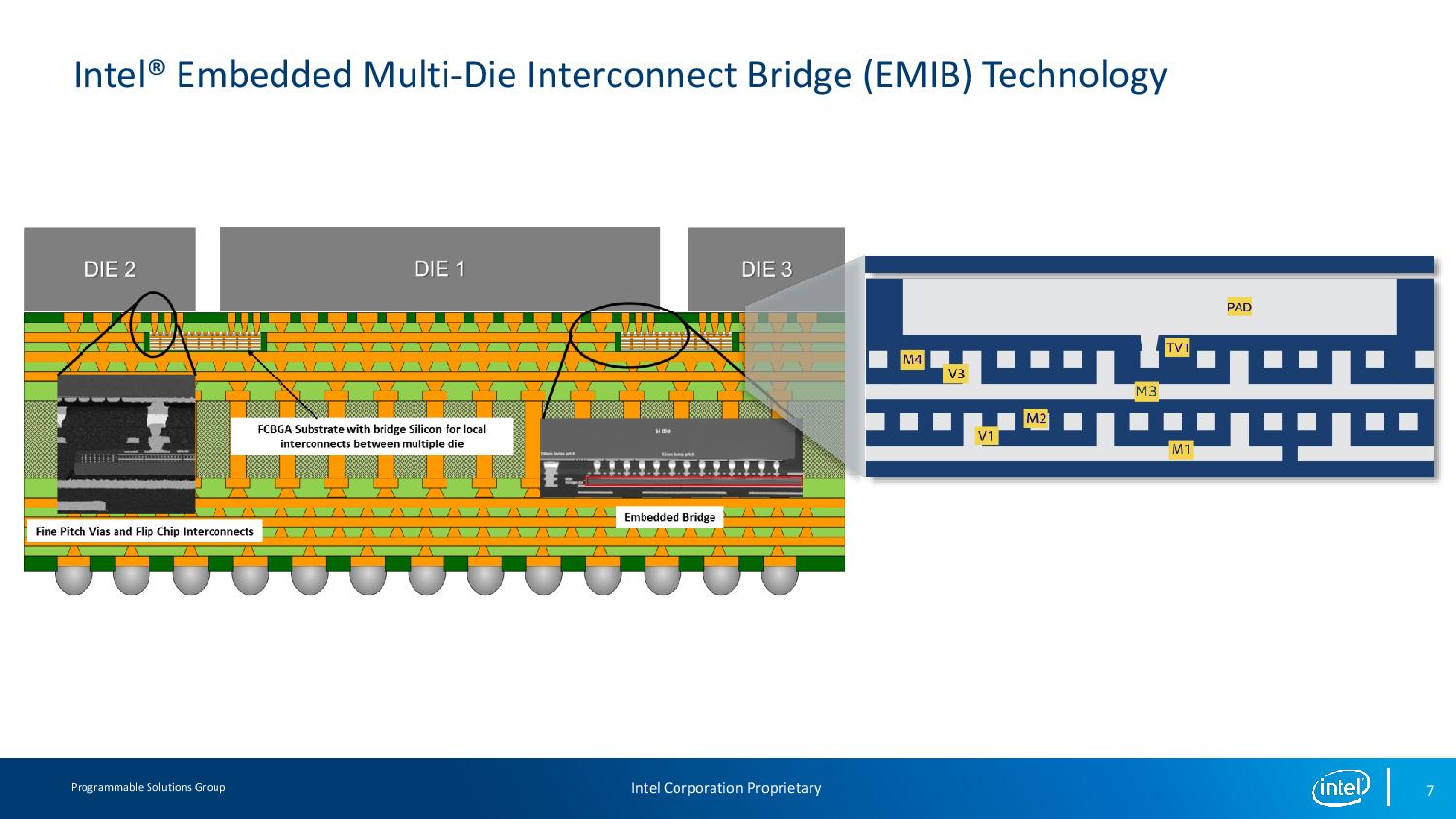
Looking at the image provided by Intel on the new product arrangement actually adds a new question or two to the bucket list. Here we have an Intel chip on the right, the AMD custom graphics in the middle, and the HBM2 chip next to it. The Intel chip is a long way away from the AMD chip, which would suggest that these two are not connected via EMIB if the mockup was accurate. The close proximity of the big chip in the middle to what looks like a HBM2 stack does suggest that it is connected via EMIB, as given by how close the chips in the Altera products are:
EMIB is being used, but it does not look like it is being used for all the chips together. It’s worth noting that neither Intel nor AMD offered pre-briefings on this announcement, so there are a lot of unanswered questions hanging around as a result.
A final thought. Apple uses a lot of Intel's 45W processors for iMacs; offering AMD graphics (Apple's preferred pro-graphics partner) into the segment that previously Intel's Crystalwell/eDRAM based products exist might be the next step on that product cycle evolution.
Source: Intel
Source: AMD
More Commentary
After an hour or two to digest, we have some new thoughts.
Firstly, judging by the wording and Intel's launch video, it can basically be confirmed that EMIB is only being used between the GPU and the HBM2. The distance between the CPU and GPU is too far for EMIB, so is likely just PCIe through the package which is a mature implementation. This configuration might also help with power dissipation if the chips are further apart.
The agreement between AMD and Intel is that Intel is buying chips from AMD, and AMD is providing a driver support package like they do with consoles. There is no cross-licensing of IP going on: Intel likely provided AMD with the IP to make the EMIB chipset connections for the graphics but that IP is only valid in the designs that AMD is selling to Intel (it's a semi-custom foundry business, these agreements are part of the job).
With Intel buying chips from AMD, it stands to reason they could be buying more than one configuration, depending on how Intel wanted to arrange the product stack. Intel could pair a smaller 10 CU design with a dual core, and a bigger 20+ CU design with a quad-core mobile processor. A couple of benchmark sources seem to believe that there is at least two configurations in Polaris-like configurations, with up to 24 CUs in the high-end model. We will obviously wait before confirming this, as Polaris is not originally built for HBM2 memory. Normally with HBM2 it requires a GPU that is designed to be fed by HBM - data management is a key operation. However, if it works 'naturally', then it should be a case of attaching the HBM2 controller IP to the GPU and away you go.
In an ideal world, it would make sense for AMD to sell Intel their Polaris designs, and for their own products say at least one generation ahead. With AMD's financial success of late, they could be in a position to do this, or Intel might be offering top dollar for the latest design. Neither company have commented on the arrangement between the two companies yet other than their press releases.
In discussions with Peter Bright from Ars Technica, we have concluded that it is likely for the Intel GPU to still keep its own integrated graphics, and the system could act in a switching graphics arrangement. This would be easy if the CPU and GPU are connected via PCIe, as all the mechanisms are in place. With the Intel integrated GPU already there, video playback would be accelerated and kept on die then sent to the display controller - it would allow the GPU and the HBM2 to power down, saving energy. If the GPU and HBM2 were kept powered up, then we would see reductions in battery life for future devices.
It has been discussed if this is a play just for Apple, given that Apple was behind Intel implementing eDRAM on its Crystalwell processors, and the latest generation of Crystalwell parts seem to be in Apple iMacs almost exclusively. That being said, Intel has stated that they have multiple partners interested in the design, and we should expect more information with devices in Q1. With Intel saying 'devices', it stands to reason that there are various OEMs waiting to work with the hardware.
As for the types of devices that we will be seeing, this one is a little confusing. Intel quoted Core-H series CPUs, which are 35W/45W parts. This also gels with comments saying that these new parts and Ryzen Mobile would not be in direct competition. However, in the demo video provided, it is clear that the potential for this design to go into thin and light notebooks like 2-in-1s and ultra-portables is on Intel's mind. Does that mean Intel is targeting 15W? Well if Intel is buying multiple configurations of chips from AMD, then strapping a dual-core i5 to 10 CU graphics part is more than plausible. If AMD is selling Intel the older Polaris design, the AMD has that advantage at least.


252 Comments
View All Comments
ZeDestructor - Tuesday, November 7, 2017 - link
Damn.. this went a tad longer than I expected...IGTrading - Tuesday, November 7, 2017 - link
I like your post mate. It is factually corect for the most part (and I say that because I didn't check every fact since most of them I know already and I see you depicted them correctly).But you present disparate facts that don't have a direct connection with our scenario of the innovation competition between AMD and Intel in the x86 space.
Reffering to that, AMD invented, developed, supported and brought to the market way more technologies than Intel which Intel initially bashed and then copied.
That's what I'm trying to say.
Copper interconnects: AMD introduces successfuly, Intel follows later without success ( 7 years of Pentium 4 based CPUs)
IMC: AMD introduces very early and successful, Intel follows much, much later
HyperTransport: AMD introduces, Intel follows much later
APUs: AMD introduces, Intel launches FIRST but with bad performance
HBM: AMD introduces with limited success, Intel copies much later
and so on ...
Intel did one thing and one thing only: x86 .
They they quiclky tried to kove away from it and failed while Cyrix taught them a hardware lesson.
Then they again tried to move away by EPIC and failed incredibly painful being beaten by AMD on the x86 side and IBM, Fujitsu, Sun, NEC on all other sides.
They tried graphics for almost a decade, lost 11 billion USD and gave up before ANY produc got to the market.
They tried paralel computing for almost 5 years now and for 5 years especially nVIDIA (but even AMD) beat them so bad that they've spent 15 billion on Altera to try and diversify a bit.
They tried competing with GloFlo and TSMC and failed miserably as a FAB.
All they've achieved was through bribery and illegal activities being sentenced in over 5 countries on 3 different continents: https://m.youtube.com/watch?v=osSMJRyxG0k
Trying to paint Intel in a decent light is hard mate :)
ZeDestructor - Tuesday, November 7, 2017 - link
*sigh*Copper interconnects: IBM beat everyone cause THEY FREAKING INVENTED IT. AND shipped it in volume with various Power ISA stuff and maybe even system/390. I believe nV and ATi GPUs were also fabbed at IBM at the time, which puts AMD anywhere from 2nd to 4th place in colume shipments of copper interconnects. Intel was perfectly fine with their 180nm-65nm nodes, it's just that NetBurst was a massive fail. Also, ignoring Pentium M there, I see, which beat the crap out of everything else on the market, both Intel and AMD, if you were willing to overclock.
HT/IMC: counterpoint: AMD weren't able to get FSB fast enough so they had to go for an IMC+HT setup. Besides, AMD is hardly the first there: all kinds of embedded chips (most notably ARM and MIPS) had IMCs for embedded and mobile devices, like routers, phones, PDAs. As I said, x86 isn't the only architecture out there.
APUs: mobile and embedded (including consoles) got there YEARS earlier than both.
HBM: Intel was about a year later there, I'll grant that.
On the x86 ISA front, Intel has led that from far more than AMD. SSE and AVX may not be as visible as x86_64, but they're equally important, especially AVX. AVX512 is twice as fast as AXV2, which is twice as fast as AVX1, which is twice as fast as SSE4, which is I believe ~3x as fast as "base" x86. This isn't the work of a company resting on their laurels, this is very deep, very serious cutting-edge engineering. Of course, the industry being convergent perf-wise means that IBM added similar stuff to POWER, and ARM did the same to some ARM cores.
As I said in my original comment, Itanium (EPIC) is a great architecture - arguably the best ISA+architecture combo ever released in the history of computing, but the launch fail, combined with the x86 platform being given a massive boost from x86_64, combined with the effectively Intel-HP only approach killed Itanium very very dead.
Graphics.. meh. AMD never even tried building a GPU from scratch like Intel - they just bought ATi for billions instead. If I had to call a company not innovative there, I'd say it's AMD, not Intel. Besides, have you even looked at how complicated building a GPU is? And all the patent licensing? Shits HARD, yo.
Parallel computing-wise, Xeon Phi is pretty cool and functional. The problem there is the nVidia/CUDA monopoly, which is stifling AMD just as much as Intel. Also, did you know that Apple was the lead company behind OpenCL that AMD joined in wholesale later when they gave up on AMD Stream SDK due to developers ignoring it in favour of CUDA?
Up until about 3 years ago, Intel fabs were strictly Intel-only. Intel wasn't even trying to compete with TSMC, GloFo and Samsung. Even now, Intel is still a ways ahead of TSMC, GloFo and Samsung in actual measurements and switching performance (some 30% denser with about 10% better perf), but them doing their own naming makes em look worse. Seriously, TSMC "12nm" is basically the exact same dimensions as TSMC "16nm FF+".. and bigger than Intel 14+ and 14++. If Intel actually opens it's fab up to all and sundry, things will get very interesting, very, very fast.
The bribery and other illegal activities while true, shouldn't undermine their technical achievements when technical achievements were achieved. Intel is still a terrible company in some respects though, I have to say (their stance on x86 licensing in particular disgusts me).
Jaybus - Tuesday, November 7, 2017 - link
IBM did indeed invent copper interconnects, but not for Power ISA stuff. The first systems shipped with CPUs using copper interconnects was the 6th gen S/390 mainframes in 1999. Matter of fact, many of the innovations in microprocessor design were scaled down mainframe concepts. Not trying to diminish Intel or AMDs efforts! The scaling down WAS the innovation. The concept of using multiple different processors combined into a single unit has long been the standard in the mainframe world, only they are implemented as MCMs (multichip modules) that have a number of central processors, clock chips, storage controllers, vector processors, specialized i/o processors, etc. Intel and AMD are now taking the heterogeneous processor design and scaling it down to fit on a single chip. Not necessarily a new concept, but definitely a huge step in the right direction. Combining an AMD GPU and Intel CPU on the same silicon is just the tip of the iceberg. Why bother with AVX when you can include a full-blown FPGA?smilingcrow - Tuesday, November 7, 2017 - link
Yet for ten years they didn't put out any decent CPUs except for a few small niches and nearly went bankrupt!IGTrading - Tuesday, November 7, 2017 - link
Yes smilingcrow ... In a way ... But not for 10 years ... More like 5 years ...Phenom II was a good chip in desktop and server and Bulldozer which had its weaksides was only launched in 2011 I think ...
So not 10 years ... Just 5 years ...
But not even 5 ... Because we have Jaguar which was extremely successful selling in hundreds of millions of consoles.
Also AMD Mullins was an absolute monster compared to Atom and this is why Intel bribed ALL the tablet makers in the world (losing 4 billion USD per year) to not make a single tablet with AMD Mullins.
So yeah ... Many amazing AMD products did not get to us, but thet doesn't mean AMD did not make "any decent CPUs" for the past 10 years.
They had them. Offered them. Intel bribed and we never got them.
patrickjp93 - Tuesday, November 7, 2017 - link
Omniscale predates Infinity Fabric by 2 years.AMD did not invent TSVs. Micron and Intel did when they invented HMC 3 years before HBM
Intel is not using a glue interconnect.
APIs which Intel helped them invent.
First with copper interconnects? Oh hell no. IBM beat both of them to it by 4 years.
No, Intel produced the first APU a full year ahead of AMD.
ironargonaut - Monday, November 6, 2017 - link
You mean like when they put a thermal switch on the core so that you wouldn't fry the part if you made a mistake or like one case I saw a heat sink (non-Intel spec) literally fell off a friends CPU when the clamp became brittle and broke. They were up to no good saving people from having to buy new processors. AMD on the other hand... copied Intel's lead after it was pointed out they had no such feature. So, save your selective memory for comment sections on the kiddie blogs where they might believe you.ZeDestructor - Tuesday, November 7, 2017 - link
You should check my looong-ass comment I wrote just above.. most of the claims he makes aren't even AMD wins...IGTrading - Tuesday, November 7, 2017 - link
For Intel it was necessary like hell, especially on their overheating Pentium 4s.AMD had the feature, the motherboard manufacturers did not implement it.
What you remember was a publicity stunt made by Tom Pabst.