The AMD 2nd Gen Ryzen Deep Dive: The 2700X, 2700, 2600X, and 2600 Tested
by Ian Cutress on April 19, 2018 9:00 AM ESTTalking 12nm and Zen+
One of the highlights of the Ryzen 2000-series launch is that these processors use GlobalFoundries’ 12LP manufacturing process, compared to the 14LPP process used for the first generation of Ryzen processors. Both AMD and GlobalFoundries have discussed the differences in the processes, however it is worth understanding that each company has different goals: AMD only needs to promote what helps its products, whereas GlobalFoundries is a semiconductor foundry with many clients and might promote ideal-scenario numbers. Earlier this year we were invited to GlobalFoundries Fab 8 in upstate New York to visit the clean room, and had a chance to interview Dr. Gary Patton, the CTO.

The Future of Silicon: An Exclusive Interview with Dr. Gary Patton, CTO of GlobalFoundries
In that interview, several interesting items came to light. First, that the CTO doesn’t necessarily have to care much about what certain processes are called: their customers know the performance of a given process regardless of the advertised ‘nm’ number based on the development tools given to them. Second, that 12LP is a series of minor tweaks to 14LPP, relating to performance bumps and improvements that come from a partial optical shrink and a slight change in manufacturing rules in the middle-line and back-end of the manufacturing process. In the past this might not have been so news worthy, however GF’s customers want to take advantage of the improved process.
Overall, GlobalFoundries has stated that its 12LP process offers a 10% performance improvement and a 15% circuit density improvement over 14LPP.
This has been interpreted in many ways, such as an extra 10% frequency at the same power, or lower power for the same frequency, and an opportunity to build smaller chips.
As part of today’s launch, AMD has clarified what the move to 12LP has meant for the Ryzen 2000-series:
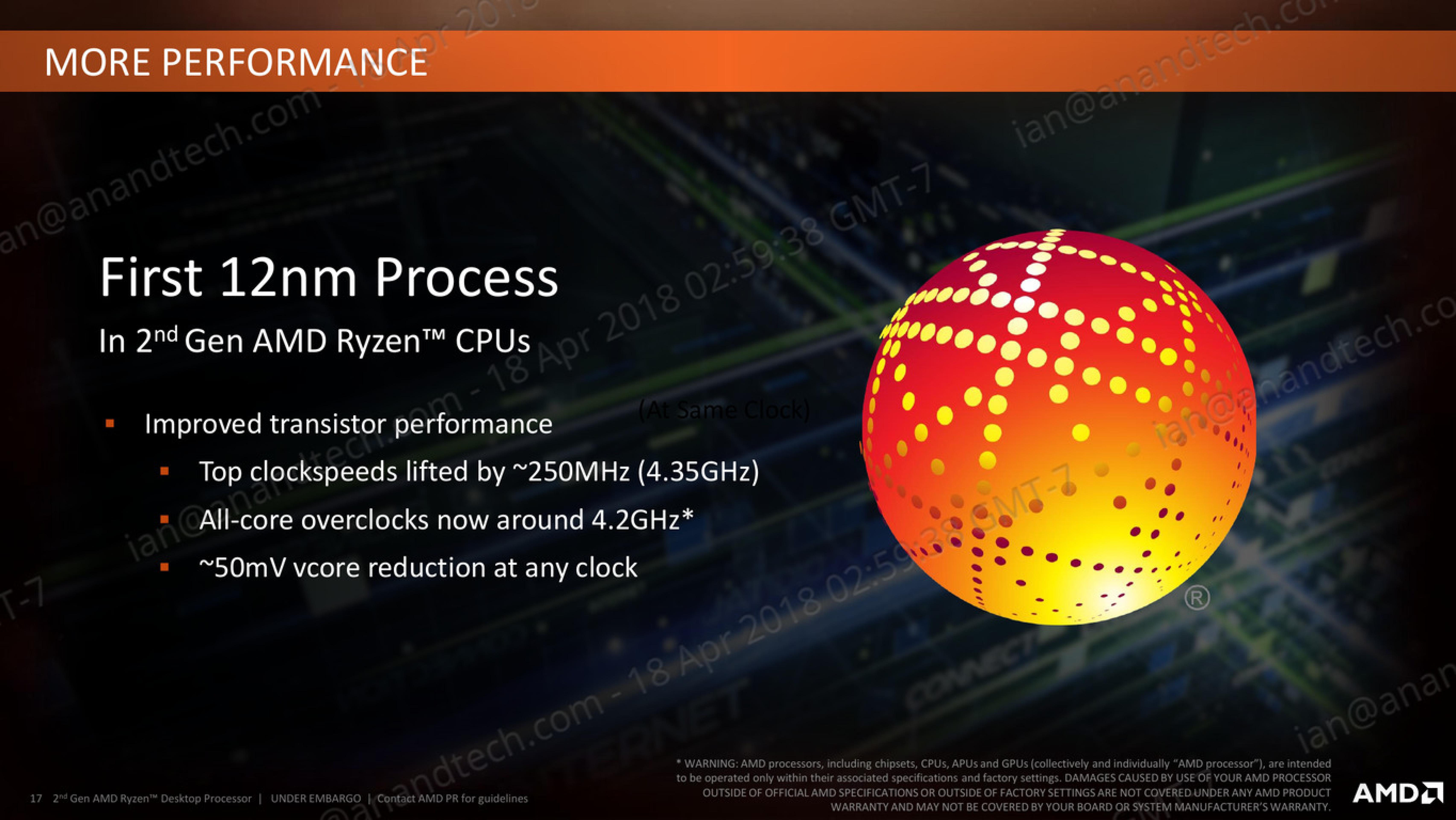
- Top Clock Speeds lifted by ~250 MHz (~6%)
- All-core overclocks around 4.2 GHz
- ~50 mV core voltage reduction
AMD goes on to explain that at the same frequency, its new Ryzen 2000-series processors draw around 11% less power than the Ryzen 1000-series. The claims also state that this translates to +16% performance at the same power. These claims are a little muddled, as AMD has other new technologies in the 2000-series which will affect performance as well.
One interesting element is that although GF claims that there is a 15% density improvement, AMD is stating that these processors have the same die size and transistor count as the previous generation. Ultimately this seems in opposition to common sense – surely AMD would want to use smaller dies to get more chips per wafer?
Ultimately, the new processors are almost carbon copies of the old ones, both in terms of design and microarchitecture. AMD is calling the design of the cores as ‘Zen+’ to differentiate them to the previous generation ‘Zen’ design, and it mostly comes down to how the microarchitecture features are laid out on the silicon. When discussing with AMD, the best way to explain it is that some of the design of the key features has not moved – they just take up less area, leaving more dark silicon between other features.
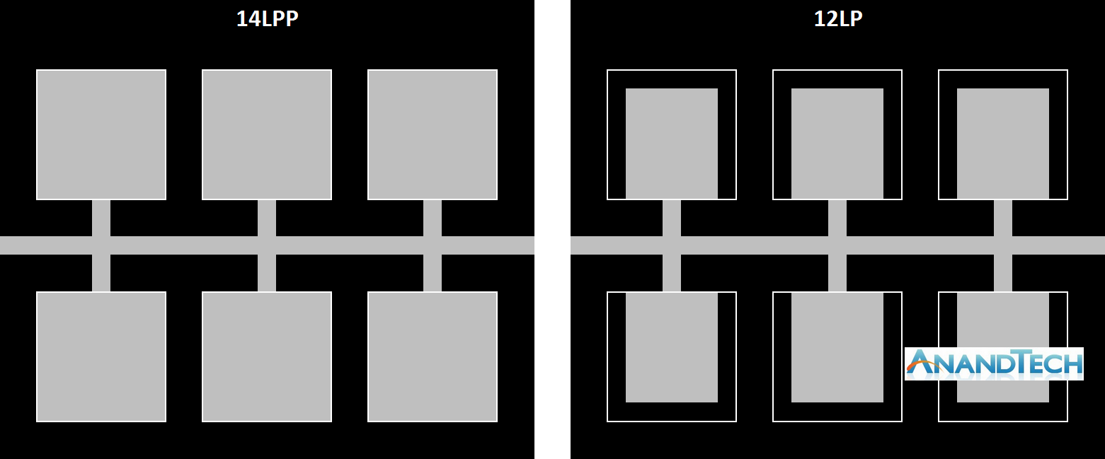
Here is a very crude representation of features attached to a data path. On the left is the 14LPP design, and each of the six features has a specific size and connects to the bus. Between each of the features is the dark silicon – unused silicon that is either seen as useless, or can be used as a thermal buffer between high-energy parts. On the right is the representation of the 12LP design – each of the features have been reduced in size, putting more dark silicon between themselves (the white boxes show the original size of the feature). In this context, the number of transistors is the same, and the die size is the same. But if anything in the design was thermally limited by the close proximity of two features, there is now more distance between them such that they should interfere with each other less.
For reference, AMD lists the die-size of these new parts as 213mm2, containing 4.8 billion transistors, identical to the first generation silicon design. AMD confirmed that they are using 9T transistor libraries, also the same as the previous generation, although GlobalFoundries offers a 7.5T design as well.
So is Zen+ a New Microarchitecture, or Process Node Change?
Ultimately, nothing about most of the Zen+ physical design layout is new. Aside from the manufacturing process node change and likely minor adjustments, the rest of the adjustments are in firmware and support:
- Cache latency adjustments leading to +3% IPC
- Increased DRAM Frequency Support to DDR4-2933
- Better voltage/frequency curves, leading to +10% performance overall
- Better Boost Performance with Precision Boost 2
- Better Thermal Response with XFR2


545 Comments
View All Comments
bryanlarsen - Thursday, April 19, 2018 - link
Just because transistors can be 15% smaller, doesn't mean that they have to be. Every IC design includes transistors of many different sizes. GF is saying that the minimum transistor size is 15% smaller than the previous minimum transistor size. And it seems that AMD chose not to use them, selecting to use a larger, higher performance transistor instead that happens to be the same size as their previous transistor.bryanlarsen - Thursday, April 19, 2018 - link
And you confirm that in the next paragraph. "AMD confirmed that they are using 9T transistor libraries, also the same as the previous generation, although GlobalFoundries offers a 7.5T design as well." So please delete your very misleading transistor diagram and accompanying text.danjw - Friday, April 20, 2018 - link
I think you are misreading that part of the article. AMD shrunk the size of the processor blocks giving them more "dark silicone" between the blocks. This allowed better thermal isolation between blocks, thus higher clocks.The Hardcard - Thursday, April 19, 2018 - link
“Cache Me Ousside, How Bow Dah?“Very low hanging fruit, yet still so delicious.
msroadkill612 - Thursday, April 19, 2018 - link
"Intel is expected to have a frequency and IPC advantageAMD’s counter is to come close on frequency and offer more cores at the same price
It is easy for AMD to wave the multi-threaded crown with its internal testing, however the single thread performance is still a little behind."
If so, why is it given such emphasis - its increasingly a corner xase benefit as game devs begin to use the new mainstream multi core platforms. Oh so recently, the norm wa probably 2 core, so that's what they coded for - THEN.
This minor advantage, compares to intel getting absolutely smashed on increasingly multi threaded apps, at any price point, is rarely mentioned in proximity, where it deserves to be in a balanced analysis.
Ratman6161 - Thursday, April 19, 2018 - link
"its increasingly a corner xase benefit as game devs begin to use the new mainstream multi core platforms" As I often do, I'd like to remind people that not all readers of this article are gamers or give a darn about games. I am one of those i.e. game performance is meaningless to me.0ldman79 - Thursday, April 19, 2018 - link
Agreed.I am a gamer, but the gaming benchmarks are nearly irrelevant at this point.
Almost every CPU (ignoring Atom) can easily feed a modern video card and keep the framerate above 60fps. I'm running an FX 6300 and I still run everything at 1080p with a GTX 970 and hardly ever see a framerate drop.
Gaming benches are somewhat less important than days gone by. Everything on the market hits the minimum requirement and then some. It's primarily fuel for the fanboys, "OMG!!! AMD sucks!!! Intel is faster at gaming!!!"
Well, considering Intel is running 200fps and AMD is hitting 175fps I'm *thinking* they're both playable.
Akkuma - Thursday, April 19, 2018 - link
Gaming + streaming benchmarks, as done by GamersNexus, are exactly the kind of relevant and important benchmarks more sites need to be doing. Those numbers you don't care about are much more important when you start trying to do streaming.Your 60fps? That isn't even what most people who game care about with high refresh rate monitors doing 144hz+. Add in streaming where you're taking a decent FPS hit and that difference between 200 and 175 fps all of a sudden is the difference between maintaining the 144hz and not.
Vesperan - Thursday, April 19, 2018 - link
Yea but.. of all the people interested in gaming, those with high refresh rate monitors and/or streaming online is what - 10% of the market? Tops?Sure the GamersNexus reviews have relevance.. to that distinct minority of people out there. Condemning/praising CPU architectures for gaming in general due to these corner cases is non-sensical.
Like Oldman79 said, damn near any of these CPUs is fine for gaming - unless you happen to be one of the corner cases.
Akkuma - Friday, April 20, 2018 - link
You're pulling a number out of thin air and building an entire argument around a made up number. 72% of steam users have 1080p monitors. What percentage of those are high refresh rate is unknown, but 120hz monitors have existed for at least 5 years now and maybe even longer. At this stage arguing around 60fps is like arguing about sound quality of cassettes today as we are long past it.