The AMD 2nd Gen Ryzen Deep Dive: The 2700X, 2700, 2600X, and 2600 Tested
by Ian Cutress on April 19, 2018 9:00 AM ESTTalking 12nm and Zen+
One of the highlights of the Ryzen 2000-series launch is that these processors use GlobalFoundries’ 12LP manufacturing process, compared to the 14LPP process used for the first generation of Ryzen processors. Both AMD and GlobalFoundries have discussed the differences in the processes, however it is worth understanding that each company has different goals: AMD only needs to promote what helps its products, whereas GlobalFoundries is a semiconductor foundry with many clients and might promote ideal-scenario numbers. Earlier this year we were invited to GlobalFoundries Fab 8 in upstate New York to visit the clean room, and had a chance to interview Dr. Gary Patton, the CTO.

The Future of Silicon: An Exclusive Interview with Dr. Gary Patton, CTO of GlobalFoundries
In that interview, several interesting items came to light. First, that the CTO doesn’t necessarily have to care much about what certain processes are called: their customers know the performance of a given process regardless of the advertised ‘nm’ number based on the development tools given to them. Second, that 12LP is a series of minor tweaks to 14LPP, relating to performance bumps and improvements that come from a partial optical shrink and a slight change in manufacturing rules in the middle-line and back-end of the manufacturing process. In the past this might not have been so news worthy, however GF’s customers want to take advantage of the improved process.
Overall, GlobalFoundries has stated that its 12LP process offers a 10% performance improvement and a 15% circuit density improvement over 14LPP.
This has been interpreted in many ways, such as an extra 10% frequency at the same power, or lower power for the same frequency, and an opportunity to build smaller chips.
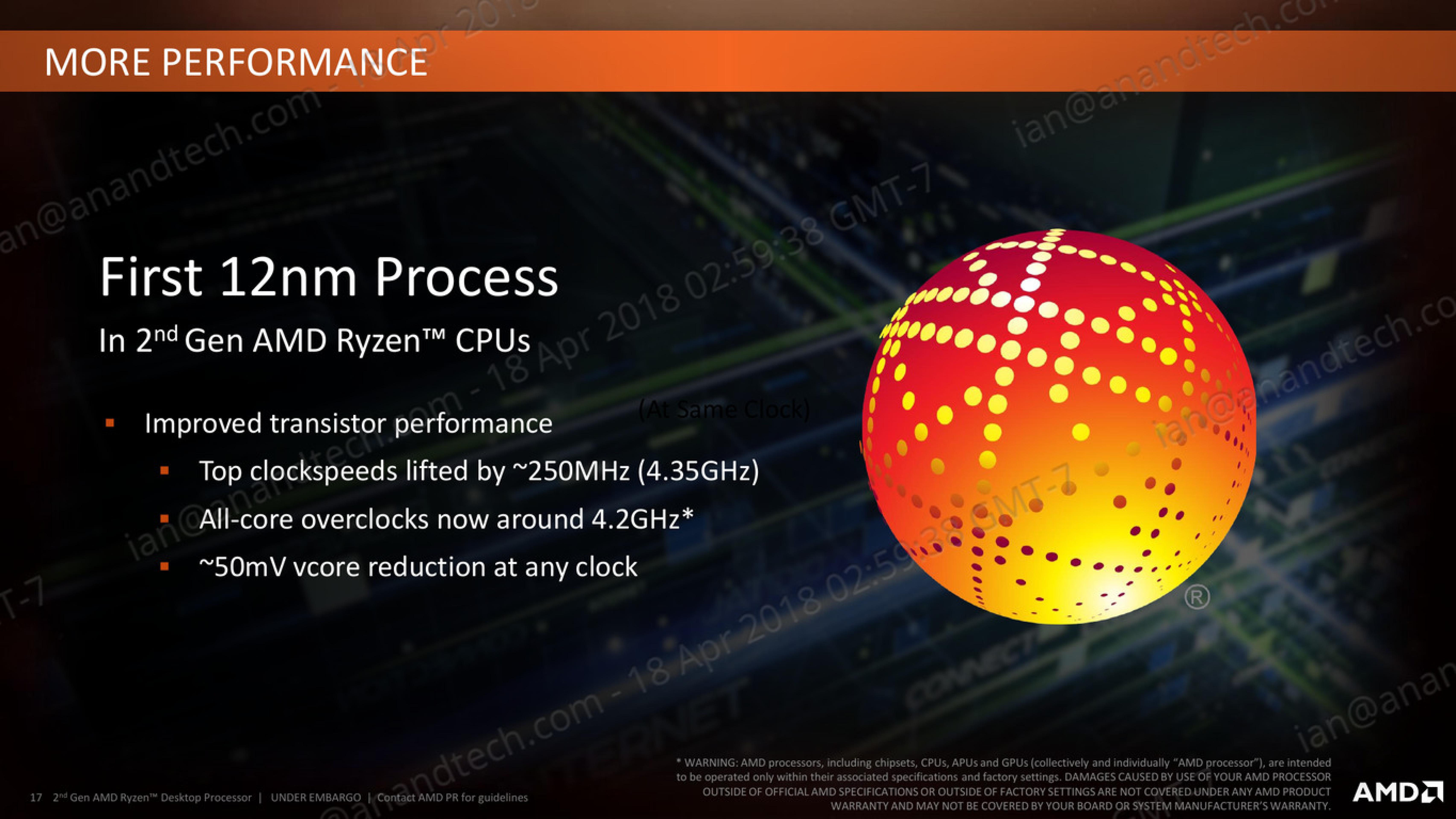
As part of today’s launch, AMD has clarified what the move to 12LP has meant for the Ryzen 2000-series:
- Top Clock Speeds lifted by ~250 MHz (~6%)
- All-core overclocks around 4.2 GHz
- ~50 mV core voltage reduction
AMD goes on to explain that at the same frequency, its new Ryzen 2000-series processors draw around 11% less power than the Ryzen 1000-series. The claims also state that this translates to +16% performance at the same power. These claims are a little muddled, as AMD has other new technologies in the 2000-series which will affect performance as well.
One interesting element is that although GF claims that there is a 15% density improvement, AMD is stating that these processors have the same die size and transistor count as the previous generation. Ultimately this seems in opposition to common sense – surely AMD would want to use smaller dies to get more chips per wafer?
Ultimately, the new processors are almost carbon copies of the old ones, both in terms of design and microarchitecture. AMD is calling the design of the cores as ‘Zen+’ to differentiate them to the previous generation ‘Zen’ design, and it mostly comes down to how the microarchitecture features are laid out on the silicon. When discussing with AMD, the best way to explain it is that some of the design of the key features has not moved – they just take up less area, leaving more dark silicon between other features.
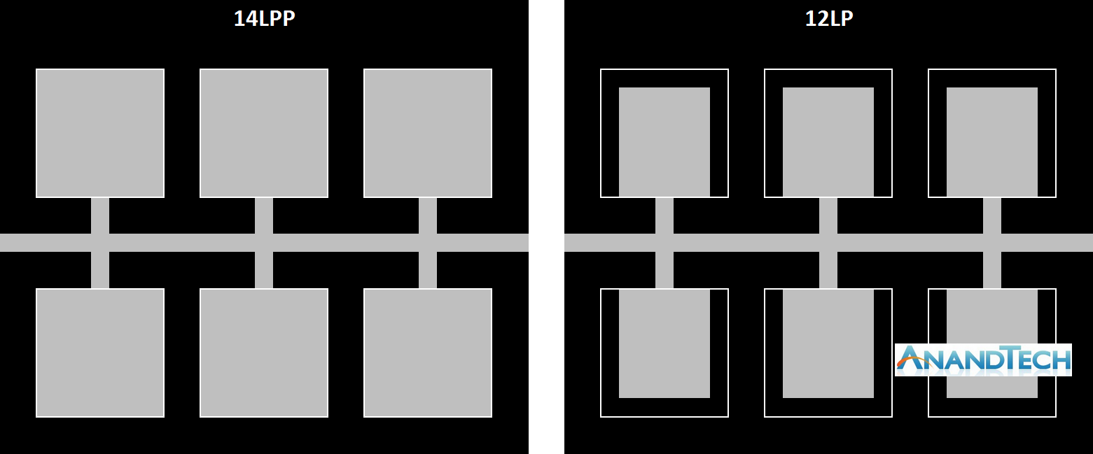
Here is a very crude representation of features attached to a data path. On the left is the 14LPP design, and each of the six features has a specific size and connects to the bus. Between each of the features is the dark silicon – unused silicon that is either seen as useless, or can be used as a thermal buffer between high-energy parts. On the right is the representation of the 12LP design – each of the features have been reduced in size, putting more dark silicon between themselves (the white boxes show the original size of the feature). In this context, the number of transistors is the same, and the die size is the same. But if anything in the design was thermally limited by the close proximity of two features, there is now more distance between them such that they should interfere with each other less.
For reference, AMD lists the die-size of these new parts as 213mm2, containing 4.8 billion transistors, identical to the first generation silicon design. AMD confirmed that they are using 9T transistor libraries, also the same as the previous generation, although GlobalFoundries offers a 7.5T design as well.
So is Zen+ a New Microarchitecture, or Process Node Change?
Ultimately, nothing about most of the Zen+ physical design layout is new. Aside from the manufacturing process node change and likely minor adjustments, the rest of the adjustments are in firmware and support:
- Cache latency adjustments leading to +3% IPC
- Increased DRAM Frequency Support to DDR4-2933
- Better voltage/frequency curves, leading to +10% performance overall
- Better Boost Performance with Precision Boost 2
- Better Thermal Response with XFR2


545 Comments
View All Comments
fallaha56 - Thursday, April 19, 2018 - link
Er look again Intel fanboisTechradar review with fully patched intel systems is showing exactly the same thing...
Spectre2 patch looks like it has a massive hit
Tropicocity - Thursday, April 19, 2018 - link
Then why do other reviews not show even near the level of performance gap between Ryzen 1 and Ryzen 2? It's not as if spectre or meltdown patches would somehow make the 2 series way better than the 1fallaha56 - Thursday, April 19, 2018 - link
XFR, ram, cooling, MCE, lots of variables hereBut the key difference is the patching and quite possibly the RAM
DearEmery - Thursday, April 19, 2018 - link
I tend to keep away from the comments here because I lack the knowledge to really contribute.I couldn't resist the urge to pop in because I'm certain this is the only time that sentence will be me boasting, when I'm reading comments from 'kill3x' and 'realistz' concerning 'hard fails'.
Follow my great example and realize your anecdote (leaving aside your 'hard fail' comprehending results and placing them in context the article hands you plenty of, assuming you read every word you should have), is right on the edge of worthless and garbage. Then read all the comments (particularly page one and two). Then come back tomorrow to get potential updates. Then go back into whatever game you were playing and be silly gooses there.
Ryan Smith - Thursday, April 19, 2018 - link
Hey Kill3x,To clarify, are you looking at the same sub-score we are, or the overall average? Our posted results are off of the first scene, Valley, as that's the most strenuous. The overall average is going to be higher, as you can see here: https://www.anandtech.com/bench/GPU16/1471
kill3x - Thursday, April 19, 2018 - link
Thank you for your reply, Ryan. Yes, this is more on point. But then again, if you mean Geothermal valley, I have different results there. The first area is Siberian wilderness with heavy snow, and I have lower results there. So a question arises about testing methods and testing scenes. Was it combat? Static? In a cave or on the top of area? All of these things affect FPS heavily. That's why the best way to review hardware in games is using scripted scenes and showing results in a video with detailed options' setup. Why didn't you guys just use ingame benchmark which 100% runs same scenes with same density? All of this looks like reviewer tried to cherrypick results in favor of Zen+. When you can't reproduce the result of a benchmark with same hardware as reviewer used is example of a bad approach and distortion of perception of your visitors.But then again, thank you, Ryan, for speaking with us and listening to our rant.
Ryan Smith - Thursday, April 19, 2018 - link
"Why didn't you guys just use ingame benchmark which 100% runs same scenes with same density?"To clarify, we do. We just use one of the scenes, and not the average of all of them. This is the same scene we've used for over a year now, since introducing this benchmark to our CPU & mobo testing suite.
kill3x - Friday, April 20, 2018 - link
Ryan, I retested Valley scene in built-in benchmark, this time with 8700k and gtx 980 Ti. I used high instead of very high, all options like on your screenshot. I got 122 FPS on valley with this settings. On 980 Ti. I'm really trying to keep this polite, but this is 20% difference on marginally weaker card. This just can't be a "gap" kind of error. These benchmarks are horribly wrong. Make your site and Ian a favor, Ryan, please consider retesting this. People are already suspect you of shill (rightfully so). Be an honest guy and just admit that a technical mistake was made, and correct it. Noone would blame you, mistakes happen. If you leave that as it is, it will be a much bigger mistake.divertedpanda - Saturday, April 21, 2018 - link
Your setup is no where near similar to theirs. You can't use your PC to Bench vs Them, and call it scientific.......kill3x - Saturday, April 21, 2018 - link
Yeah my setup's is nowhere near similar to theirs, and still my results are 20% better on 2 different CPUs. That kinda puts credibility of their review to zero, with all my respect to Ryan. The only goal was to put Ryzen 1 and CFL-S CPUs in a bad light, so people will buy new Ryzen 2 CPUs and suddenly find out that its capability's are not that huge.