Intel's Interconnected Future: Combining Chiplets, EMIB, and Foveros
by Dr. Ian Cutress on April 17, 2019 8:00 AM EST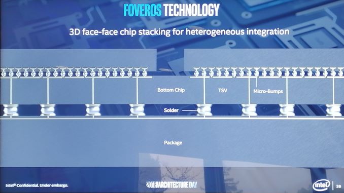
While Intel works on getting its main manufacturing process technology on track, it is spending just as much time and effort in researching and developing the rest of the chip ecosystem and how it is all connected. On a call with Intel's process and product team, the company confirmed a few details about how Intel is pushing the boundaries of new technologies with its upcoming high profile graphics products.
An Insight into Intel's Strategy on Chiplets and Packaging
In a call with Intel last week, we spoke with Ramune Nagisetty, the Director of Intel’s Process and Product Integration, to discuss Intel’s strategy with regard to chiplets and packaging technologies. Ramune has spent over twenty years at Intel, working in areas such as transistor definition for 65nm, Intel Labs for technical strategy and wearables, and most recently as heading up Intel’s chiplet strategy for product integration. Ramune focuses on the art of the chiplet or the packaging in its own right, rather than the specific technologies it goes into, and it was an enlighting discussion.

Ramune Nagisetty
The story around chiplets is going to be a cornerstone of the semiconductor market for the next generation, being able to provide smaller silicon for specific tasks and connecting them together. Chiplets form the basis of Intel’s current Stratix 10 FPGA product line, and the future of Intel Agilex, as well as consumer products like Kaby Lake G with its HBM chiplet for fast high-speed memory. How Intel integrates its own chiplets, with the company confirming it is working on migrating its AI portfolio into chiplet form factors, as well as other third party IP, is going to be an important strategy going forward. The art of connecting chiplets, however, is all in the packaging. Intel has several technologies of its own that it uses.
EMIB, Foveros, Interposers: Connect the Data
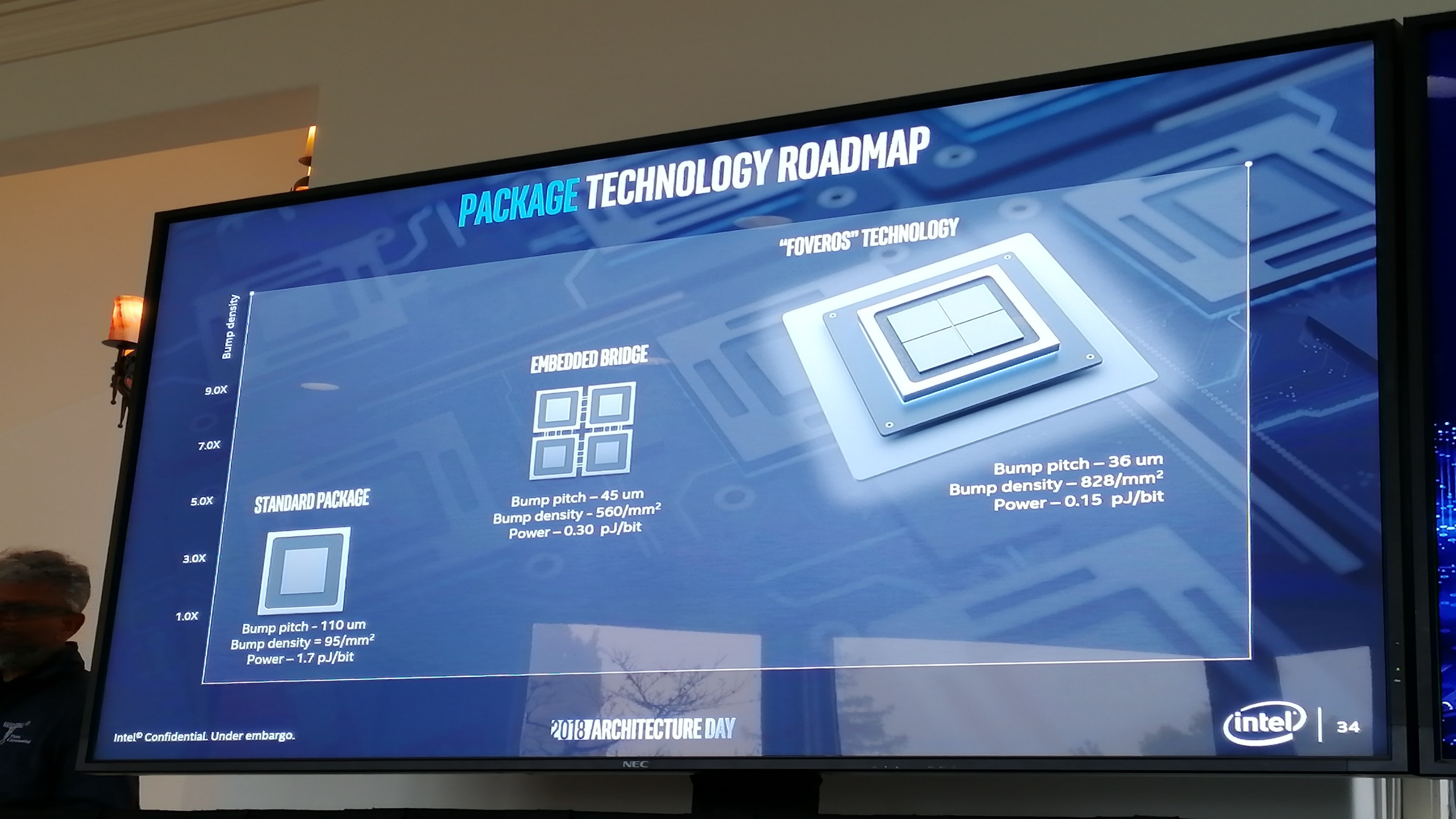
Intel’s Embedded Die Interconnect Bridge ‘EMIB’ has been a talking point for a couple of years now. Because certain high-performance chiplet designs require high-bandwidth links with many more traces than traditional organic chip packaging can support, there is a need for more exotic means to build these dense connections. The 'brute force' solution here is a silicon interposer, essentially stacking chips on top of a large, 'dumb' silicon die that's in place solely for routing purposes.
With EMIB however, rather than using a full silicon interposer, Intel equips a substrate with just a small embedded silicon connection, allowing a host chip and a secondary chiplet to connect together with high bandwidth and small distances. This technology is currently in Intel’s FPGAs, connecting the FPGA to memory or transceivers or third-party IP, or in Kaby Lake-G, connecting the Radeon GPU to on-package high bandwidth memory.
Intel has also uses full interposers in its FPGA products, using it as an easier and quicker way to connect its large FPGA dies to high bandwidth memory. Intel has stated that while large interposers are a catch-all situation, the company believes that EMIB designs are a lot cheaper than large interposers, and provide better signal integrity to allow for higher bandwidth. In discussions with Intel, it was stated that large interposers likely work best for powerful chips that could take advantage of active networking, however HBM is overkill on an interposer, and best used via EMIB.
Akin to an interposer-like technology, Foveros is a silicon stacking technique that allows different chips to be connected by TSVs (through silicon vias, a via being a vertical chip-to-chip connection), such that Intel can manufacture the IO, the cores, and the onboard LLC/DRAM as separate dies and connect them together. In this instance, Intel considers the IO die, the die at the bottom of the stack, as a sort of ‘active interposer’, that can deal with routing data between the dies on top. Ultimately the big challenges with a multi-die strategy come with in thermal constraints of the dies used (so far, Intel has demonstrated a 1+4 core solution in a 12x12mm package, called Lakefield), as well as aligning known good die for TSV connections.
Discussing Strategy: Intel's Engineering Approach
Intel is clearly committed to its chiplet strategy where it currently stands with FPGAs, bringing other aspects of Intel’s technology to the platform (such as AI), and developing features such as EMIB into it. Ramune made it clear that if Intel’s customers have their own third party IP in use with the FPGA, they will need to either provide the EMIB capable chiplets themselves or work with Intel’s foundry business to enable them, and then the packaging will be done solely at Intel. While Intel has offered connectivity standards to the open market, the specific EMIB technology that Intel uses is designated a product differentiation, so customers will have to engage with Intel in order to see their IP in the packaged product.
![]()
When it comes to chip stacking technologies like Foveros, Ramune reiterated some of the key areas of the technology that are being worked on, such as thermal limitations as well as die size and efficient stacking. One of the key changes was described as ensuring that when dies are stacked that known good dies (i.e. those that pass yield tests) are used, which requires bare die testing before assembly. Some of Intel’s previous development processes have needed to be adjusted in order to assist for technologies like Foveros and products like Lakefield, as well as other products in the future. Ramune did state that Intel has not specifically looked into advanced cooling methods for Foveros type chips, but did expect work in this field over the coming years, either internally or externally.
When discussing products in the future, one critical comment did arise from our conversation. This might have been something we missed back at Intel’s Architecture Day in December last year, but it was reiterated that Intel will be bringing both EMIB and Foveros into its designs for future graphics technologies. As one might imagine, no further comment was offered regarding the scale, thermal performance, interconnect integration, or anything along those lines, but it is clear that Intel is looking into multi-die graphics technologies. One might by cynical and state that Intel is already using both EMIB and Foveros in graphics today: Kaby G uses EMIB, and Lakefield has an integrated Gen11 graphics on Foveros. However these are two separate products, and our takeaway from the conversation was that both of these technologies might be on a singular product in the future.
This could take many different forms. A central control chip connected by EMIB to compute chips, using Foveros to increase the amount of onboard cache each of the control chips has. Compute chips could be daisy chained by EMIB. The control chip could need a central DRAM repository, either by Foveros or via EMIB. These technologies are like Lego – go build a spaceship, or a ferris wheel, or a GPU.
Splitting GPUs into chiplets isn’t a new idea in the realm of ideas, however it is a concept that is difficult to conceive. One of the key areas of shuffling data around a GPU is bandwidth – the other is latency. In a graphics scenario, the race is on to get a low frame rendering time, preferably below 16.67 milliseconds, which allows for a refresh rate of 60 Hz to have a full display frame inserted on every refresh cycle. With the advent of variable refresh displays this has somewhat changed, however the main market for graphics cards, gamers, is heavily reliant on quick refresh rates and high frame rates from their graphics. With a multi-chip module, the manufacturer has to consider how many hops between dies the data has to perform from start to finish – is the data required found directly connected to the compute chip, or does it have to cross from the other side of the design? Is the memory directly stacked, or is there an intrapackage connection? With different memory domains, can the data retain its concurrency through the mathematical operations? Is there a central management die, or do each of the compute chiplets manage their own timing schema? How much of the per-chiplet design comes from connectivity units compared to compute units?
Ultimately this sort of design will only win out if it can compete on at least two fronts of the triad of performance, cost, or power. We already know that multi-die environments typically require a higher power budget than a monolithic design due to the extra connectivity, as seen with multi-die CPU options in the market, so the chiplets will have to take advantage of smaller process nodes in order to eliminate that deficit. Luckily, small chiplets are easier to manufacturer on small process nodes, making it a potential cost saving over big monolithic designs. Performance will depend on the architecture, both for raw compute, as well as the interconnect between the chips.
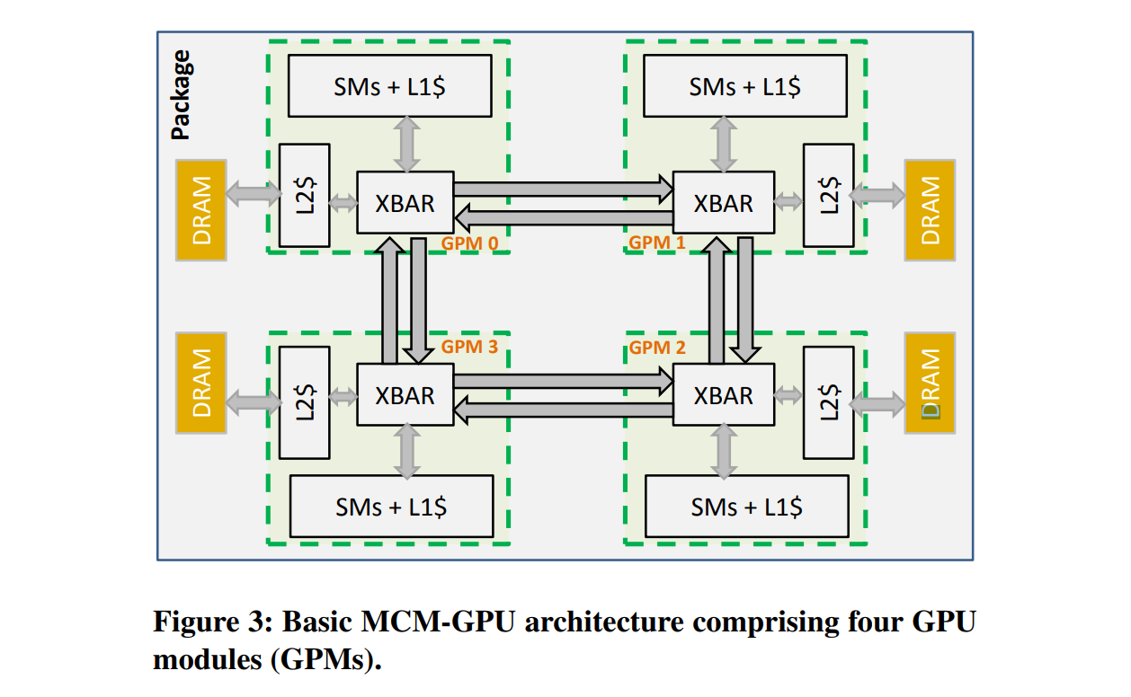
NVIDIA MCM GPU Diagram from ISC '17
We have seen several research papers discuss the concept of a multi-die graphics solution, such as this one from NVIDIA, and you can bet your bottom dollar that everyone involved in high performance graphics and high performance compute is looking at it. Given the fact that a compute platform has fewer restrictions than a graphics platform, we might expect to see a multi-die solution there first.
The other element to our discussion was a reaffirmation of comments made previously by Dr. Murthy Renduchintala, Intel’s Chief Engineering Officer and Group President of the Technology, Systems, Architecture and Client Group. Ramune stated that chiplet technology and packaging technologies are designed to run asynchronously to Intel’s current manufacturing processes. Ultimately the goal here is to apply the technologies to the process currently available, rather than fixing development and tying development to a single node strategy. As we’ve seen with how Intel’s 10nm development has progressed, this disaggregation of product and technology is going to be an important step in Intel’s future.
What We Do Know About Intel's Xe GPU Line
Intel has already stated that after Gen11 graphics, which will be featured in its future Ice Lake consumer processors paired with the Sunny Cove microarchitecture, that we will see its Xe graphics products come to the market. Xe will range from integrated graphics all the way up to enterprise compute acceleration, covering through the consumer graphics and gaming markets as well.
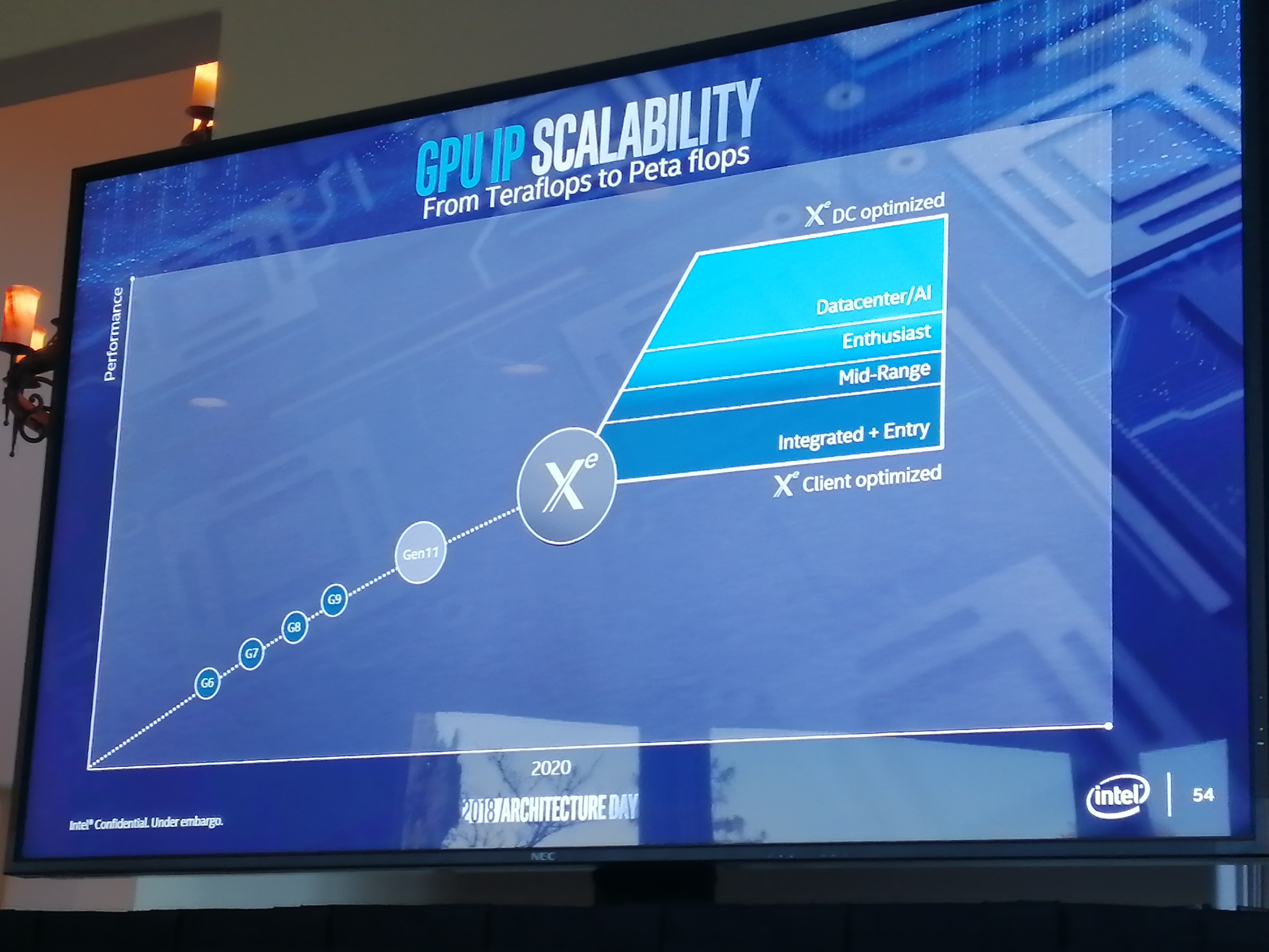
Intel stated at the time that the Xe range will be built on two different architectures, one of which is called Arctic Sound, and the other has not yet been made public. The goal is to create a platform for Xe relating the hardware, the software, the drivers, the platform, and the APIs all into a single mission, which Intel calls 'The Odyssey'. Introducing EMIB and Foveros technologies as part of the Xe strategy seems to be very much part of Intel's plan, and it will be interesting to see how it develops.
Beyond Intel's Core Technologies
Intel’s recent push into graphics technology is well known. The company has hired Raja Koduri from AMD, Jim Keller from Tesla, Chris Hook from AMD, and a number of high profile tech journalists and AMD’s GPU marketing manager to help develop its discrete graphics offerings. Even as of a couple of days ago the company wasn't quite done with their hiring spree, picking up GlobalFoundries' Corporate Communications director to assist in its manufacturing process and packaging technologies disclosures. While 10nm is being fixed, the company is clearly trying to get the attention onto its new product areas, and its new capabilities – we’ve seen new packaging technologies and core configurations at Intel’s Tech Summit in December, and an array of enterprise products other than CPUs at the company’s recent Data Centric launch event. As Intel develops both its chiplet strategy and its packaging implementations, we should expect the expertise to permiate through Intel's product portfolio where it expects to help those products gain an advantage. Lakefield is a key example of this, offering Core, Atom, and Gen11 functionality in a tiny chip and under 7W for small form factor devices.

Lakefield, built with Foveros
Many thanks to Ramune Nagisetty and her team for the call last week, and some insight into a part of Intel we’ve not normally had contact with before. I’m glad that Intel is starting to open up more into new areas like this, and hope that it continues in the future.
Related Reading
- Hot Chips: Intel EMIB and 14nm Stratix 10 FPGA
- Intel Launches Stratix 10 TX: Leveraging EMIB with 58G Transceivers
- Intel Agilex: 10nm FPGAs with PCIe 5.0, DDR5, and CXL
- Intel's Architecture Day 2018: The Future of Core, Intel GPUs, 10nm, and Hybrid x86
- CES 2019 Quick Bytes: Intel’s 10nm Hybrid x86 Foveros Chip is Called Lakefield
- Intel’s Keynote at CES 2019: 10nm, Ice Lake, Lakefield, Snow Ridge, Cascade Lake
- Intel’s Enterprise Extravaganza 2019: Launching Cascade Lake, Optane DCPMM, Agilex FPGAs, 100G Ethernet, and Xeon D-1600
- Intel to Create new 8th Generation CPUs with AMD Radeon Graphics with HBM2 using EMIB


117 Comments
View All Comments
mode_13h - Monday, April 22, 2019 - link
Focusing on EMIB misses the point. The point is you have a situation where all GPU cores from all dies are equidistant from all memory controllers. You're forcing the memory controller die to have a giant, multi-TB/sec crossbar. If you read any coverage of NVSwitch, you'd know it already burns a significant amount of power, and what you're talking about is even a multiple of that level of bandwidth.https://www.anandtech.com/show/12581/nvidia-develo...
According to https://www.nextplatform.com/2018/04/13/building-b...
"NVSwitch consumes less than 100 watts per chip."
Granted, a good amount of that is to drive the NVLink signals further distances than required for in-package signalling, but a non-trivial amount must be for the switching, itself.
To scale *efficiently*, the way to go is NUMA hardware + NUMA-aware software. This is the trend we've been seeing in the industry, over the past 2 decades. And it applies *inside* a MCM as well as outside the package, particularly when you're talking about GPU-scale bandwidth numbers. The only reason 7 nm EPYC can get away with it is because its total bandwidth requirements are far lower.
ats - Tuesday, April 23, 2019 - link
GPUs already have giant multi-TB/sec crossbars. How do you think they already connect the shader blocks to the memory controller blocks?NVSwitch is not even close to equiv to what we are creating here. We're doing a on package optimized interconnect and simply moving what would of been a massive xbar in a monolithic GPU into a separate die connecting to a bunch of smaller dies that are effectively shader blocks just like an Nvidia SM. You are grossly mixing technologies here. NVLink is a Meter+ external FR4 interconnect, it has basically nothing in common with an on package interconnect.
NVSwitch power should be almost all link based. I've actually designed switch/routers that have shipped in silicon in millions of devices, they don't actually take up that much power.
And no, NUMA doesn't make much sense for a GPU system. It significantly increases the overheads for minimal to no benefit. NUMA isn't a goal, it is a problem. Always has been always will be. If you don't have to go down that path, and you don't for GPUs, then you don't do it. We do it for CPUs because we need to scale coherently across multiple packages, which is not and has never been a GPU issue.
mode_13h - Wednesday, April 24, 2019 - link
> GPUs already have giant multi-TB/sec crossbars. How do you think they already connect the shader blocks to the memory controller blocks?There are obviously different ways to connect memory controllers to compute resources, such as via ring and mesh topologies. In Anandtech's Tonga review, they seem to call out Tahiti's use of crossbar as somewhat exceptional and costly:
"it’s notable since at an architectural level Tahiti had to use a memory crossbar between the ROPs and memory bus due to their mismatched size (each block of 4 ROPs wants to be paired with a 32bit memory channel). The crossbar on Tahiti exposes the cards to more memory bandwidth, but it also introduces some inefficiencies of its own that make the subject a tradeoff."
...
"The narrower memory bus means that AMD was able to drop a pair of memory controllers and the memory crossbar"
https://www.anandtech.com/show/8460/amd-radeon-r9-...
Also, reduction in the width of its intra-SMX crossbars is cited in their Maxwell 2 review as one of the keys to its doubling of perf/W over Kepler:
https://www.anandtech.com/show/8526/nvidia-geforce...
> NUMA isn't a goal, it is a problem. ... If you don't have to go down that path, ... then you don't do it.
No debate there. Nobody wants it for its own sake - people do it because it scales. Crossbars do not. To feed a 4-chiplet GPU, you're probably going to need 4 stacks of HBM2, which would seem to mean 32-channels (assuming 128 bits per channel). So, we're probably talking about something like a 32x32 port crossbar. Or take GDDR6, which uses 16-bit channels, meaning a memory data bus 512 bits wide would also have 32 channels. Nvidia's TU102 uses 384-bit, so I figure a proper multi-die GPU architecture should be capable of surpassing that.
One issue is that you're assuming GPUs don't already have some form of NUMA. Even CPUs, like Intel's previous-generation HCC Xeon dies and their current-gen server dies have memory controllers distributed throughout their topology in a way that limits connectivity andincreases latency non-uniformly. Why wouldn't they have just used a crossbar, if they're as cheap as you claim?
But the real win NUMA can offer is to keep non-shared memory accesses local. So, you don't burn power shuffling around more data than necessary, you don't risk excessive bank conflicts, and (bonus) you don't need enormous, hot switches with enough bandwidth to handle all of your memory traffic.
The only reason not to consider NUMA for what's essentially a supercomputer in a package is what Wang cites, which is that ISVs have gotten used to treating graphics cores as SMP nodes. So, you've got to either bring them along, or devise a NUMA architecture that behaves enough like SMP that their existing codebase doesn't take a performance hit.
ats - Wednesday, April 24, 2019 - link
WRT why don't CPUs use a xbar....Because their traffic patterns are fundamentally different than GPUs. GPUs don't have a lot to any cross communication between computational resources. Shader Block0 doesn't really care what Shader Block1 is doing, what memory it is updating, etc. Communication is basically minimal to the point that they generally have a separate special system to allow that communication in the rare cases it is required so that the requirement doesn't impact the primary path. In contrast, CPU's computational resources are in constant communication with each other. They are always maintaining global coherence throughout the entire memory and cache stack.
GPUs basically don't have non-shared memory access per se. That's what presents all the complexities with multi-gpu setups. Shader block0 is just as likely to need to access memory blockA or blockB as shader block1. For CPUs, there are plenty of workloads that as long as they maintain coherence, don't have a lot of overlap or competition for given memory regions (and designs like AMD's original EPIC/Ryzen design do best on these effectively shared nothing workloads).
GPUs fundamentally need UMA like access for graphics workloads.
mode_13h - Wednesday, April 24, 2019 - link
> GPUs don't have a lot to any cross communication between computational resources.That might be true of GPUs from a decade ago, but AMD's GCN has globally-coherent L2 and optionally-coherent L1 data cache.
http://developer.amd.com/wordpress/media/2013/06/2...
> Shader Block0 doesn't really care what Shader Block1 is doing, what memory it is updating, etc.
That's precisely the case for NUMA, in GPUs.
> GPUs basically don't have non-shared memory access per se. That's what presents all the complexities with multi-gpu setups.
Actually, the complexities with multi-GPU setups are largely due to the lack of cache coherency between GPUs and the orders of magnitude longer latencies and lower communication bandwidth than what we're talking about. It's no accident that NVLink and AMD's Infinity Fabric both introduce cache coherency.
> GPUs fundamentally need UMA like access for graphics workloads.
The term of art for which you're reaching would be SMP. You want all compute elements to have a symmetric view of memory. Unified Memory Architecture typically refers to sharing of a common memory pool between the CPU and GPU.
https://en.wikipedia.org/w/index.php?title=Unified...
ats - Thursday, April 25, 2019 - link
Go ahead an write a program that relies on inter shader coherence and see how that works for you...No it isn't the case for NUMA, because they all want access to all of memory, they just want read access. Make it NUMA and you'll be link limited in no time.
SMP is symmetrical multi processor. It is a term of art that means that the computational units are the same. It does not actually describe memory access granularity and complexity of the system. NUMA/UMA are the correct terms for referring to memory access granularity and locality.
mode_13h - Saturday, April 27, 2019 - link
> Go ahead an write a program that relies on inter shader coherence and see how that works for you...The same is true for multi-core CPUs. At least GPUs' deeper SMT implementation can keep shader resources from sitting idle, as long as there's enough other work to be done.
If current GPU shader programming languages had something akin to OpenCL's explicit memory hierarchy and work group structure, it would be easier for the runtime to allocate shared resources and schedule their usage closer to each other. That would be a big enabler for GPUs to go NUMA. That said, you can't eliminate global communication - you just need to reduce it to within what the topology can handle.
> No it isn't the case for NUMA, because they all want access to all of memory, they just want read access.
I don't know why you think CPUs are so different. Most software doesn't use core affinity, and OS schedulers have long been poor at keeping threads and memory resources together. Efficient scaling only happens when software and hardware adapt in a collaborative fashion. OpenCL was clearly a recognition of this fact.
Also, GPUs already sort of have the problem you describe, with ever narrower memory channels. The 16-bit channels of GDDR6 could easily get over-saturated with requests. The GPU shader cores just see this as more latency, which they're already well-equipped to hide.
> SMP is symmetrical multi processor. It is a term of art that means that the computational units are the same. It does not actually describe memory access granularity and complexity of the system.
Centralized memory is fundamental to the definition of SMP.
"Symmetric multiprocessing (SMP) involves a multiprocessor computer hardware and software architecture where two or more identical processors are connected to a single, shared main memory, have full access to all input and output devices, ..."
Smell This - Friday, April 19, 2019 - link
It remains to be seen as to whether AMD can pull this out.
They have danced around unified memory and cache coherency. Bringing it all together in a heterogeneous arch is the holy grail. The good news is AMD has been building for this moment for almost ten years, from the fusion APUs with SIMD/AVX 'graphic engines' to chiplet designs with independent I/O. This. Is. Hard. Stuff. We've come quite a-ways from the fusion 'onion and garlic' days.
Bank collisions, cache thrashing, etc, are the bad, old days of NUMA and page faults. Hopefully, Rome (and improved IOMMU) will incrementally move the ball forward toward a heterogeneous unified memory between cores/chiplets/bank groups, etc. Otherwise, we're stuck in a brute-force mindset.
Smell This - Friday, April 19, 2019 - link
Bring back bank 'swizzling' ?? Is that still a thing? :)mode_13h - Saturday, April 20, 2019 - link
The Rome approach won't scale. GPUs have far higher memory bandwidth requirements than CPUs. Nvidia's not stupid. They went with an EPYC (gen 1)-like architecture for good reasons.