SK Hynix Announces 3.6 Gbps HBM2E Memory For 2020: 1.8 TB/sec For Next-Gen Accelerators
by Ryan Smith on August 12, 2019 10:00 AM EST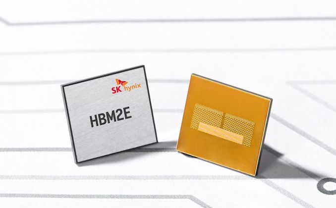
SK Hynix this morning has thrown their hat into the ring as the second company to announce memory based on the HBM2E standard. While the company isn’t using any kind of flash name for the memory (ala Samsung’s Flashbolt), the idea is the same: releasing faster and higher density HBM2 memory for the next generation of high-end processors. Hynix’s HBM2E memory will reach up to 3.6 Gbps, which as things currently stand, will make it the fastest HBM2E memory on the market when it ships in 2020.
As a quick refresher, HBM2E is a small update to the HBM2 standard to improve its performance, serving as a mid-generational kicker of sorts to allow for higher clockspeeds, higher densities (up to 24GB with 12 layers), and the underlying changes that are required to make those happen. Samsung was the first memory vendor to announce HBM2E memory earlier this year, with their 16GB/stack Flashbolt memory, which runs at up to 3.2 Gbps. At the time, Samsung did not announce a release date, and to the best of our knowledge, mass production still hasn’t begun.
Not to be left behind, SK Hynix is now also readying their own HBM2E memory. In terms of performance, SK Hynix says that their memory will be able to clock at up to 3.6 Gbps/pin, which would give a full 1024-pin stack a total of 460GB/sec of memory bandwidth, and in the process the lead for HBM2E memory speeds. And for more advanced devices which employ multiple stacks (e.g. server GPUs), this means a 4-stack processor could be paired up with as much as 1.84TB/sec of memory bandwidth, a massive amount by any measure. Meanwhile their capacity is doubling, from 8 Gb/layer to 16 Gb/layer, allowing a full 8-Hi stack to reach a total of 16GB. It’s worth noting that the revised HBM2 standard actually allows for 12-Hi stacks, for a total of 24GB/stack, however we’ve yet to see anyone announce memory quite that dense.
Given SK Hynix’s announcement, it’s interesting to note just how quickly HBM2 memory speeds have ramped up here: HBM2 vendors could barely do 1.9 Gbps 24 months ago, and now we’re looking at a near doubling of memory speeds in 3 years. This is a rather significant gain in a short period of time, especially with only a minor revision to the HBM2 spec being required. That said, I remain curious as to how SK Hynix (and Samsung) are going to deal with the heat of an 8-Hi stack running at those clocks; the HBM design philosophy is wide-and-slow, and 3.6 Gbps arguably isn’t so slow.
With their HBM2E memory set to go into mass production in 2020, SK Hynix expects the new memory to be used on “supercomputers, machine learning, and artificial intelligence systems that require the maximum level of memory performance.” All of these are distinctly high-end applications where HBM2 is already being heavily used today, so HBM2E is a natural extension to that market. At the same time, it’s also a reflection of the price/margins that HBM2 carries. HBM2 has remained (stubbornly) high-priced well after its release – a situation that memory manufacturers seem to be perfectly content with – and we’re not expecting HBM2E to change that. So expect to see SK Hynix’s HBM2E memory remain the domain of servers and other high-end equipment.
Source: SK Hynix


23 Comments
View All Comments
stadisticado - Monday, August 12, 2019 - link
People need to remember that HBM2 is a datacenter product. These things are hundreds of dollars a unit for 8-hi stacks. People hoping for an affordable GPU with even two of these stacks integrated are in dreamland.darkswordsman17 - Monday, August 12, 2019 - link
Its expensive but its not that expensive. Plus if you used it as the system memory, it'd cut out DRAM cost, while having big performance uptick (pair 16GB HBM2 with like 128GB of NAND - where the NAND could come close to DDR4 speeds with HBM2 as the NAND cache), and you'd get both much larger memory space as well as much faster memory speed (speaking of total system, think of the HBM2 being like a huge CPU/GPU cache, with the NAND being equivalent of DRAM but larger in size and non-volatile to boot).My point being, if you built a system around using HBM, the cost would be less of an issue, and would bring bigger benefits than just using it for say the GPU. It'd also enable more compact systems. But it would require developing new platform(s), although I think AMD should be looking at that due to how OEMs have been slow to support their products. AMD could make reference designs and then sell complete boards to OEMs (who put it in their own chassis, and then do the support part of things).
For AMD, they could maybe take the I/O die and put it on an interposer with the HBM, and then connect to CPU and GPU chips out from there. I don't know if they could FAB the HBM themselves too (maybe even integrate it right into the I/O die so it might not need interposer even)?
darkswordsman17 - Monday, August 12, 2019 - link
This is a nice development.I've posted this in the forums, but I wish AMD would develop a new platform, that would be like a high end PC version of consoles. It'd have CPU chiplets, GPU chiplets, and replace the system memory with HBM (which would function like a huge L3 cache). The HBM could also work as the buffer for NAND (they could put some amount onboard, where it'd mitigate any potential memory limitations - i.e. 16GB of HBM system memory for cost reasons where the onboard NAND could have similar to DRAM speeds but larger capacity; then they'd have PCIe 4.0 capable slots for SSD expansion for storage). It'd also let them easily do unified memory. It'd be good for gaming (which would let them translate a lot of development for the consoles to PC) but I think would really fly for workstations.
It'd also let them be less constrained by the socket (so for instance they could release APU systems that have two CPU chiplets and a large GPU chip, without being limited like they are by AM4 in both power and packaging size). I could see them doing something like 1-6 CPU chiplets, where the'd have small NUC like boxes for single CPU chiplet APU setups, but then have a mainstream one that could be integrated into laptops, all-in-ones, and SFF systems (plus sell as stuff like Steamboxes and Windows versions of that), then 3-6 chiplet ones for workstations (with options for multiple GPU chiplets). The number of HBM stacks would be based on the CPU chiplets (matching that number, where they could go for different stack heights and different speeds as well).
It also would let them bypass OEMs (who have been slow to support AMD platforms, and when they do often do silly stuff like use single channel memory or other things to cheap out). Heck, we still don't have Threadripper workstations (unless you built your own).