Intel Next-Gen 10-micron Stacking: Going 3D Beyond Foveros
by Dr. Ian Cutress on August 14, 2020 2:30 PM EST_678x452.jpg)
One of the issues facing next-generation 3D stacking of chips is how to increase the density of the die-to-die interface. More connections means better data throughput, reducing latency and increasing bandwidth between two active areas of silicon that might be manufactured at different process nodes. There’s also a consideration for power and thermal hotspots as well. Intel has been developing its own physical interconnect topologies, most of which we’ve covered in detail before, such as the Embedded Multi-Die Interconnect Bridge (EMIB) that allows 2D expansion and Foveros die-to-die 3D staking that enables vertical expansion. As part of Intel’s Architecture Day 2020, we have a glimpse into Intel’s future with hybrid bonding.
There are several holistic metrics to measure how ‘good’ an interconnect can be; the two that are easiest to understand are density of connections (bump density) and energy (how much energy it takes to transfer a bit).
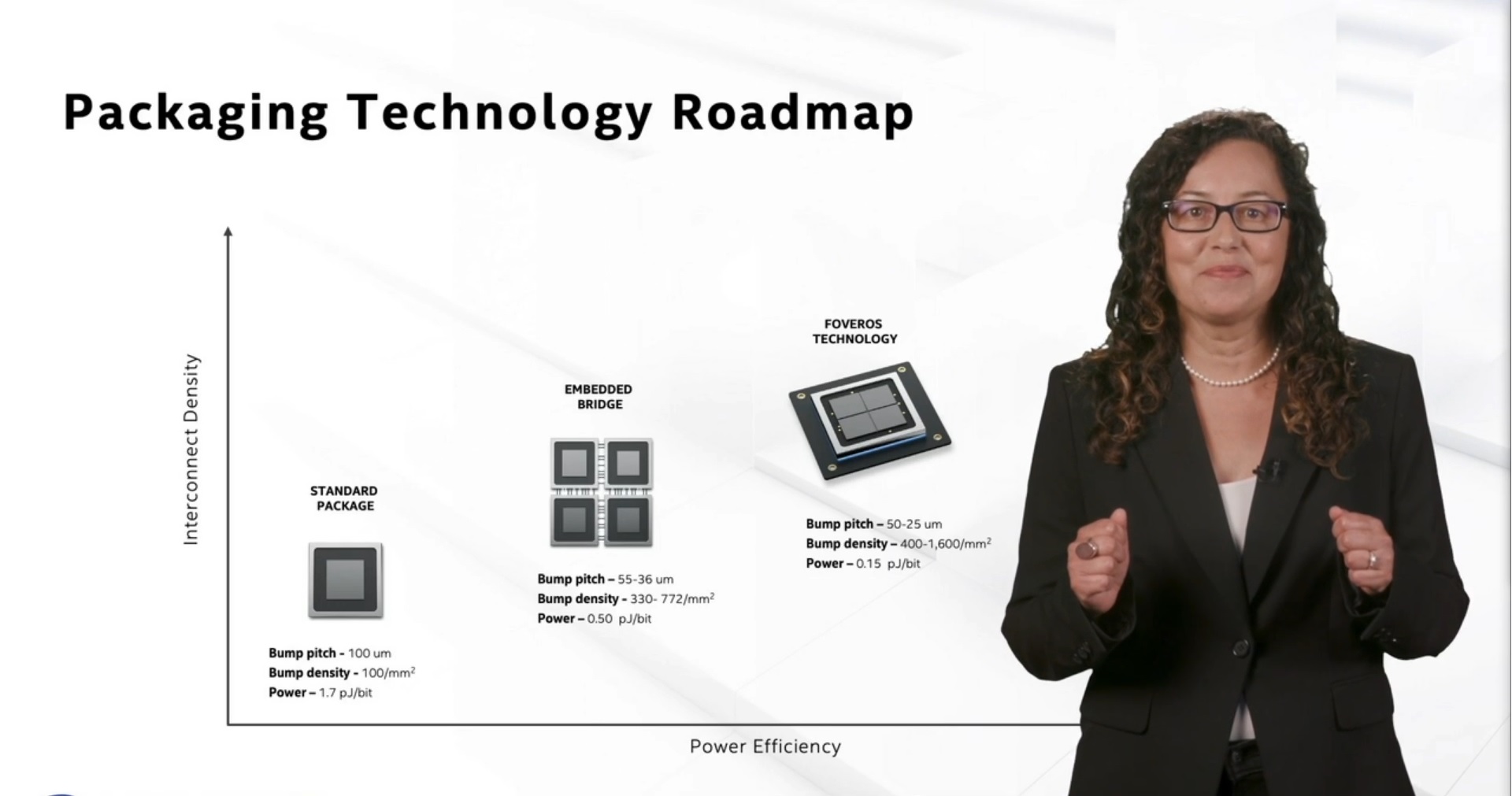
Intel's Ramune Nagisetty showcasing current packaging technologies at Intel
Intel’s own slides show us that EMIB’s bump density is good for ~400 per square millimeter, with a power of 0.50 picojoules per bit transferred. Foveros takes that a step further, supporting 400-1600 bumps per square millimeter, and an average power of 0.15 picojoules per bit transferred.
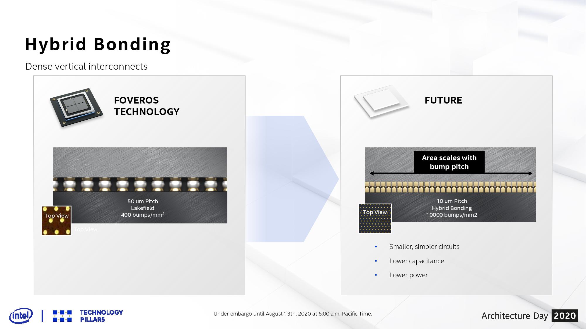
The next era of ‘Hybrid Bonding’ that Intel is going towards improves both metrics by around a factor of 3-10. The new test chips that Intel has just got back into the lab, involving stacked SRAM, goes towards the 10000 bumps per square millimeter range, with a power under 0.05 picojoules per bit. According to Intel this allows for smaller and simpler circuits, with lower capacitance and better efficiency. Nothing to be said about yields however!
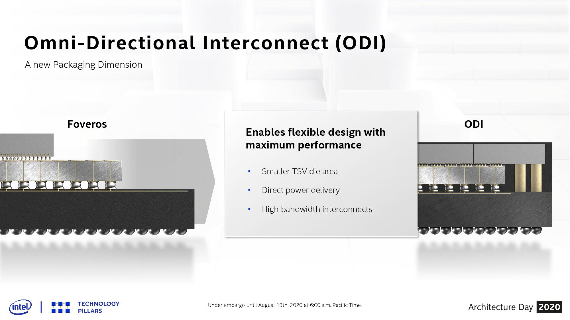
With these new bonding and stacking technologies, the question always becomes one of thermals, and how Intel might stack two performance-related bits of silicon together. In the discussions as part of Architecture Day, Intel stated that these stacked designs require having all layers designed together, rather than independently, in order to manage the electrical and thermal characteristics. As far as Intel sees it, the most power hungry layer is required to go on the top of the stack for the time being, which obviously means that the power connections have to either rise up through the lower layers, or there has to be some form of cantilevered situation where power connections can happen off the edge of the bonding – Intel calls this technology ODI, to support different sized silicon layers.
With the future of high performance and high efficiency computing coming to a head with new packaging technologies, finding the right way of going forward is ever critical. For a context on timeline, Intel’s Ramune Nagisetty has stated that Foveros was patented back in 2008, but it took nearly a decade for the process to become physically viable at scale and high-enough yielding for a product to come to market.
Related Reading
- An Interconnected Interview with Intel’s Ramune Nagisetty: A Future with Foveros
- Intel: Lakefield in 2020, Possible 5G on Foveros
- Intel’s Xe for HPC: Ponte Vecchio with Chiplets, EMIB, and Foveros on 7nm, Coming 2021
- Hot Chips 31 Live Blogs: Intel Lakefield and Foveros
- Intel's Interconnected Future: Combining Chiplets, EMIB, and Foveros
- The Intel Lakefield Deep Dive: Everything To Know About the First x86 Hybrid CPU

_thumb.jpg)
_575px_thumb.jpg)
_carousel_thumb.jpg)
_carousel_thumb.jpg)
_thumb.jpg)


31 Comments
View All Comments
randomTechSpec - Friday, August 14, 2020 - link
"[...] with a power of 0.50 petajoules per bit transferred.", must be a really power hungry chip.Joking aside, pJ means pico Joule (PJ would be Peta Joule).
LiKenun - Friday, August 14, 2020 - link
Still not enough energy to create a kugelblitz black hole with a Schwartzschild radius bigger than the radius of a proton…azfacea - Saturday, August 15, 2020 - link
of course not. what were you thinking ?? my farts often measure more than several Peta Joules.azfacea - Saturday, August 15, 2020 - link
BTW its not my fault there is no delete/edit button.Santoval - Saturday, August 15, 2020 - link
Enough however to power 9 - 10,000 thousand homes for a full year.YB1064 - Saturday, August 15, 2020 - link
It comes with Avengers packaging, so it must be good!rahvin - Friday, August 14, 2020 - link
Stacking is such a dead end because it concentrates all the heat into a smaller area and spreads that heat to additional layers with all the negative consequences.Chiplet designs like AMD is doing is the only way multichip systems are going to work efficiently IMO.
whatthe123 - Friday, August 14, 2020 - link
Doesn't seem like its meant to scale outwards. More like they're able to stack low power draw segments below the high power draw segment, so rather than all the heat working upwards most of it is already at the top. Seems like it might work but I don't think it's comparable to chiplets in yield and full cores per package.DanNeely - Friday, August 14, 2020 - link
Exactly, the main advantage of vertical stacking is that it can offer much higher bandwidth between dies than horizontally connected dies. Which is probably why they've started by stacking stuff on top of cache chips. It lets them stack another level of cache with each block of CPU cores, and they've still got Foveros to do horizontal connections similar to AMD chiplets to ramp up the total number of cores.But because each stacked chiplet is made of two dies not one, they can cram twice as many CPU cores into each; reducing the number of NUMA domains (or have double the absolute number of cores) and making it easier for software to scale up.
lmcd - Friday, August 14, 2020 - link
Ignoring that it's a smaller package size, which is a huge advantage for the design.