AMD Zen 3 Ryzen Deep Dive Review: 5950X, 5900X, 5800X and 5600X Tested
by Dr. Ian Cutress on November 5, 2020 9:01 AM ESTSection by Andrei Frumusanu
The New Zen 3 Core: Front-End Updates
Moving on, let’s see what makes the Zen3 microarchitecture tick and how detail on how it actually improves things compared to its predecessor design, starting off with the front-end of the core which includes branch prediction, decode, the OP-cache path and instruction cache, and the dispatch stage.
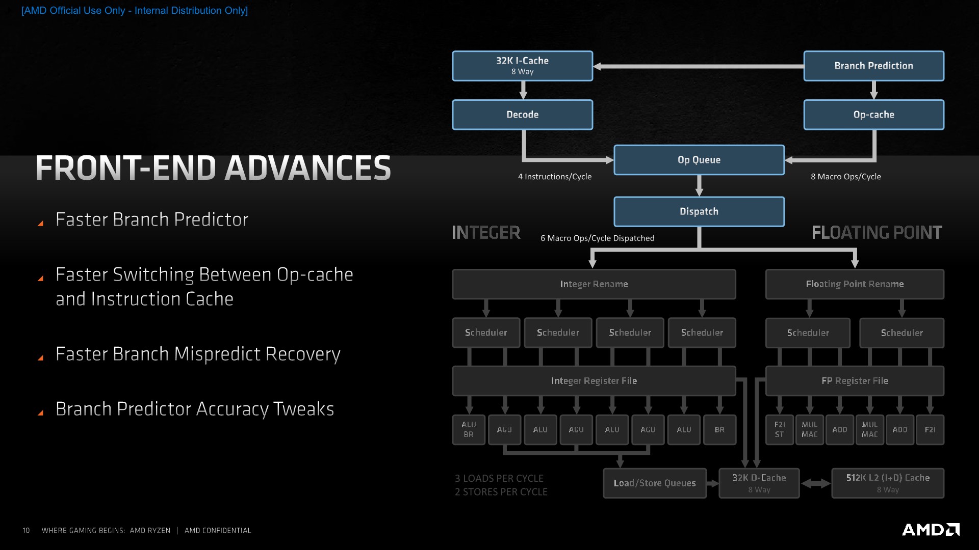
From a high-level overview, Zen3’s front-end looks the same as on Zen2, at least from a block-diagram perspective. The fundamental building blocks are the same, starting off with the branch-predictor unit which AMD calls state-of-the-art. This feeds into a 32KB instruction cache which forwards instructions into a 4-wide decode block. We’re still maintaining a two-way flow into the OP-queue, as when we see instructions again which have been previously decoded, they are then stored in the OP-cache from which they can be retrieved with a greater bandwidth (8 Mops/cycle) and with less power consumption.
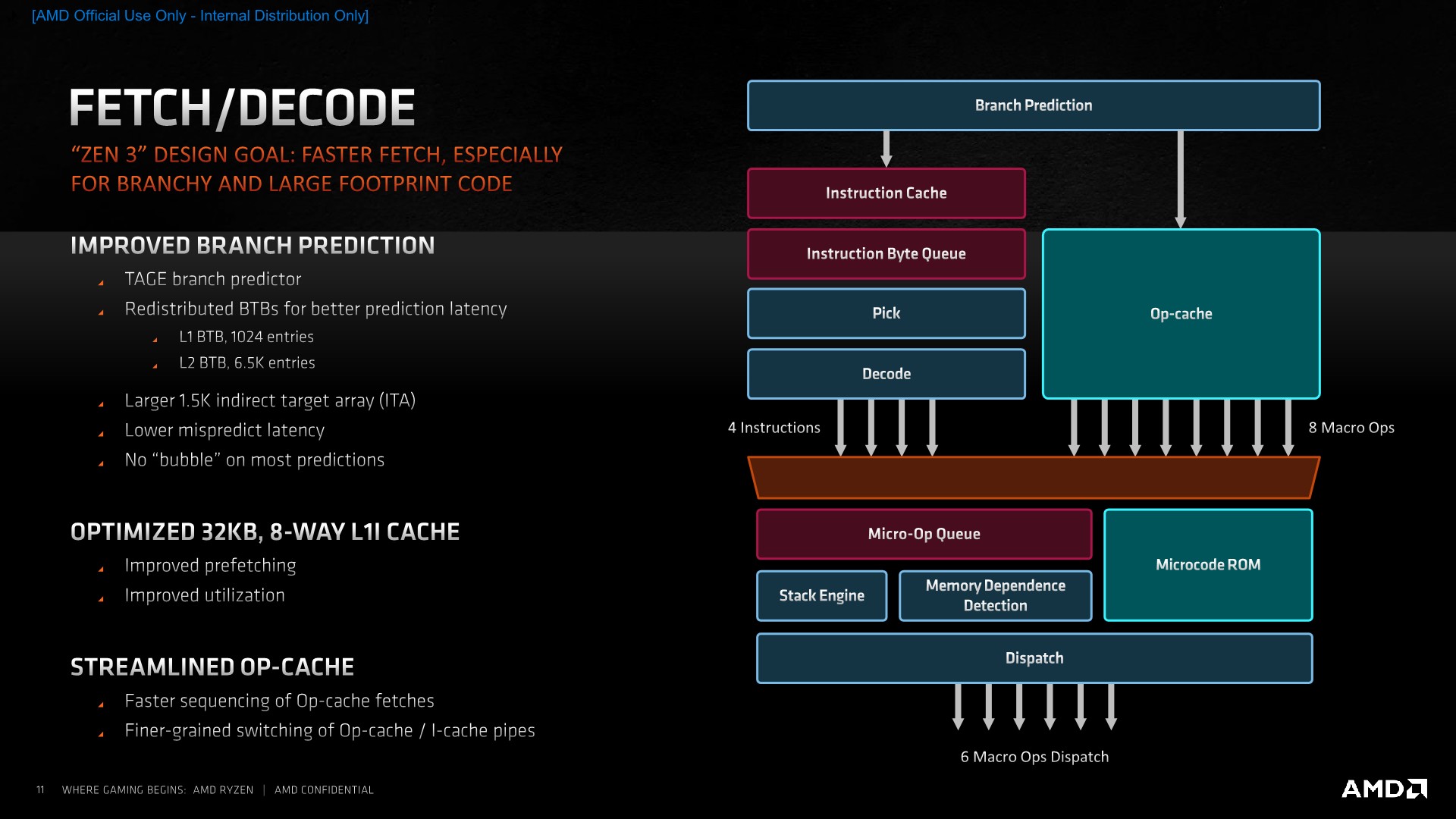
Improvements of the Zen3 cores in the actual blocks here include a faster branch predictor which is able to predict more branches per cycle. AMD wouldn’t exactly detail what this means but we suspect that this could allude to now two branch predictions per cycle instead of just one. This is still a TAGE based design as had been introduced in Zen2, and AMD does say that it has been able to improve the accuracy of the predictor.
Amongst the branch unit structure changes, we’ve seen a rebalancing of the BTBs, with the L1 BTB now doubling in size from 512 to 1024 entries. The L2 BTB has seen a slight reduction from 7K to 6.5K entries, but allowed the structure to be more efficient. The indirect target array (ITA) has also seen a more substantial increase from 1024 to 1536 entries.
If there is a misprediction, the new design reduces the cycle latency required to get a new stream going. AMD wouldn’t exactly detail the exact absolute misprediction cycles or how faster it is in this generation, but it would be a more significant performance boost to the overall design if the misprediction penalty is indeed reduced this generation.
AMD claims no bubbles on most predictions due to the increased branch predictor bandwidth, here I can see parallels to what Arm had introduced with the Cortex-A77, where a similar doubled-up branch predictor bandwidth would be able to run ahead of subsequent pipelines stages and thus fill bubble gaps ahead of them hitting the execution stages and potentially stalling the core.
On the side of the instruction cache, we didn’t see a change in the size of the structure as it’s still a 32KB 8-way block, however AMD has improved its utilisation. Prefetchers are now said to be more efficient and aggressive in actually pulling data out of the L2 ahead of them being used in the L1. We don’t know exactly what kind of pattern AMD alludes to having improved here, but if the L1I behaves the same as the L1D, then adjacent cache lines would then be pulled into the L1I here as well. The part of having a better utilisation wasn’t clear in terms of details and AMD wasn’t willing to divulge more, but we suspect a new cache line replacement policy to be a key aspect of this new improvement.
Being an x86 core, one of the difficulties of the ISA is the fact that instructions are of a variable length with encoding varying from 1 byte to 15 bytes. This has been legacy side-effect of the continuous extensions to the instruction set over the decades, and as modern CPU microarchitectures become wider in their execution throughput, it had become an issue for architects to design efficient wide decoders. For Zen3, AMD opted to remain with a 4-wide design, as going wider would have meant additional pipeline cycles which would have reduced the performance of the whole design.
Bypassing the decode stage through a structure such as the Op-cache is nowadays the preferred method to solve this issue, with the first-generation Zen microarchitecture being the first AMD design to implement such a block. However, such a design also brings problems, such as one set of instructions residing in the instruction cache, and its target residing in the OP-cache, again whose target might again be found in the instruction cache. AMD found this to be a quite large inefficiency in Zen2, and thus evolved the design to better handle instruction flows from both the I-cache and the OP-cache and to deliver them into the µOP-queue. AMD’s researchers seem to have published a more in-depth paper addressing the improvements.
On the dispatch side, Zen3 remains a 6-wide machine, emitting up to 6-Macro-Ops per cycle to the execution units, meaning that the maximum IPC of the core remains at 6. The Op-cache being able to deliver 8 Macro-Ops into the µOp-queue would serve as a mechanism to further reduce pipeline bubbles in the front-end – as the full 8-wide width of that structure wouldn’t be hit at all times.
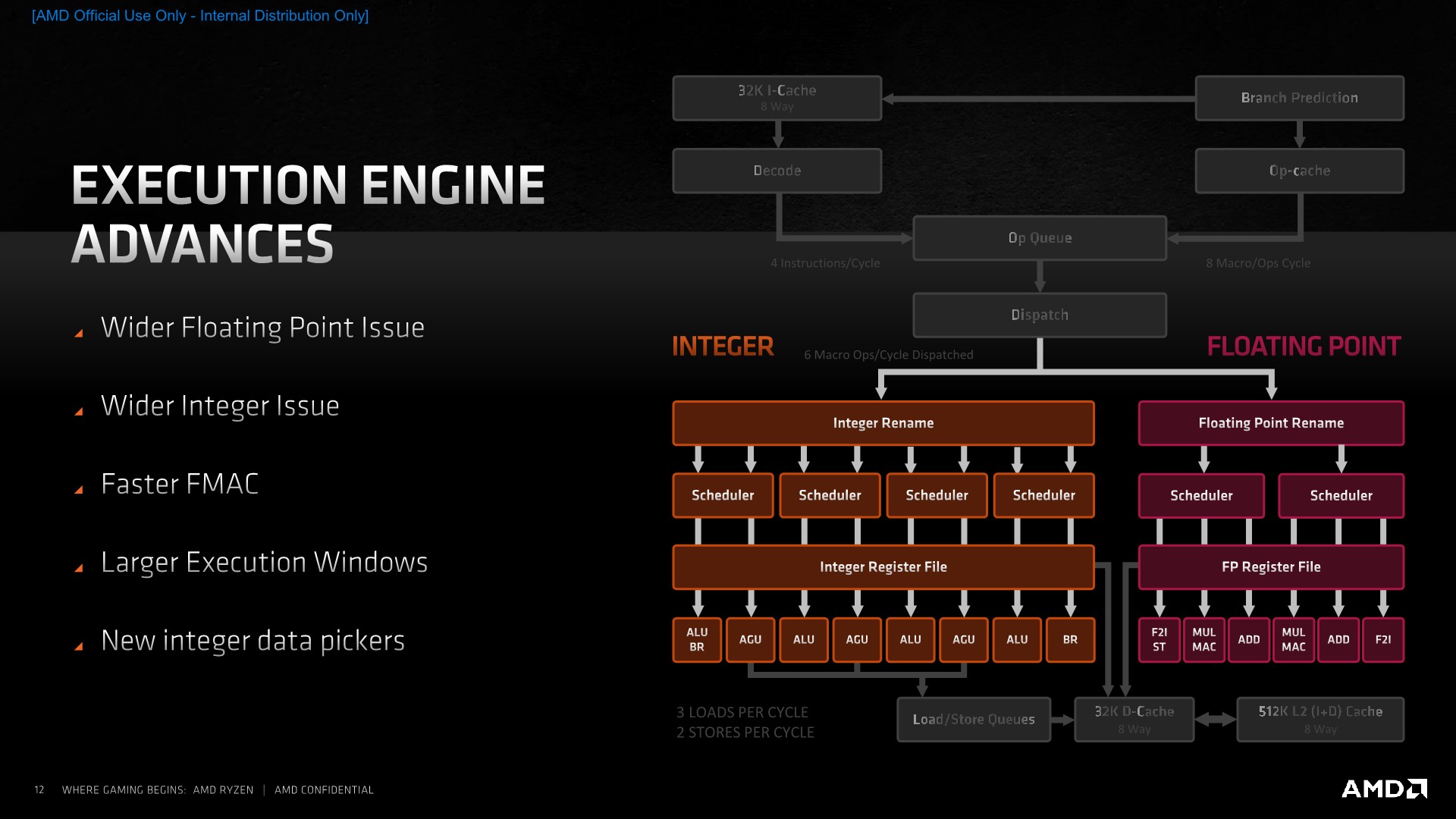
On the execution engine side of things, we’ve seen a larger overhaul of the design as the Zen3 core has seen a widening of both the integer and floating-point issue width, with larger execution windows and lower latency execution units.
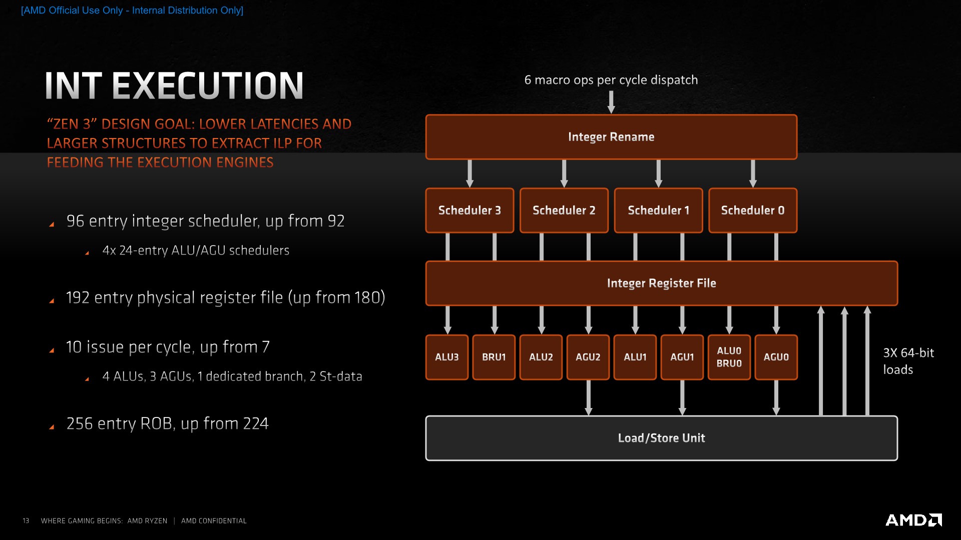
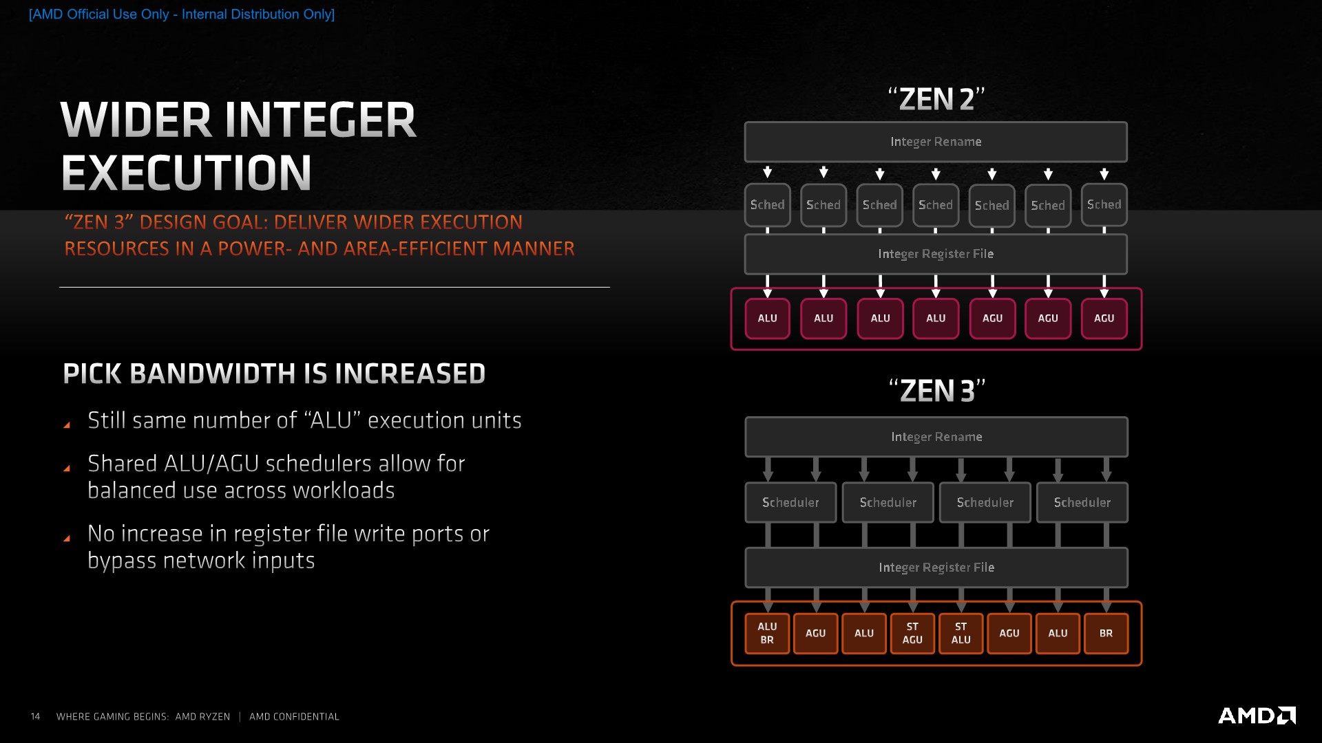
Starting off in more detail on the integer side, the one larger change in the design has been a move from individual schedulers for each of the execution units to a more consolidated design of four schedulers issuing into two execution units each. These new 24-entry schedulers should be more power efficient than having separate smaller schedulers, and the entry capacity also grows slightly from 92 to 96.
The physical register file has seen a slight increase from 180 entries to 192 entries, allowing for a slight increase in the integer OOO-window, with the actual reorder-buffer of the core growing from 224 instructions to 256 instructions, which in the context of competing microarchitectures such as Intel’s 352 ROB in Sunny Cove or Apple giant ROB still seems relatively small.
The overall integer execution unit issue width has grown from 7 to 10. The breakdown here is that while the core still has 4 ALUs, we’ve now seen one of the branch ports separate into its own dedicated unit, whilst the other unit still shares the same port as one of the ALUs, allowing for the unshared ALU to dedicate itself more to actual arithmetic instructions. Not depicted here is an additional store unit, as well as a third load unit, which is what brings us to 10 issue units in total on the integer side.
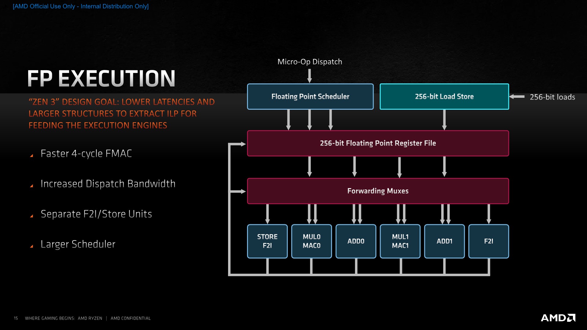
On the floating-point side, the dispatch width has been increased from 4 µOps to 6 µOps. Similar to the integer pipelines, AMD has opted to disaggregate some of the pipelines capabilities, such as moving the floating point store and floating-point-to-integer conversion units into their own dedicated ports and units, so that the main execution pipelines are able to see higher utilisation with actual compute instructions.
One of the bigger improvements in the instruction latencies has been the shaving off of a cycle from 5 to 4 for fused multiply accumulate operations (FMAC). The scheduler on the FP side has also seen an increase in order to handle more in-flight instructions as loads on the integer side are fetching the required operands, although AMD here doesn’t disclose the exact increases.


339 Comments
View All Comments
lightningz71 - Friday, November 6, 2020 - link
With the switch to DDR5 coming, there is a need to update the IO die anyway. They could move to a previous node bulk process like TSMC 10nm or Samsung's 8nm and reduce pin count for just three CCDs and manage three CCDs and one IO die in a package well enough. Given that the next CCDs will be on N5P, power draw should come down for those as well, enabling them to stay in the same envelope.lmcd - Monday, November 9, 2020 - link
Samsung's 8nm is provably undesirable for high-volume parts though. I'd argue going the other way, pick a low power node and see if you can get the chiplet architecture in high-end laptop and desktop APU SKUs. That would push their release cadence ahead to same timeframe as desktop and absolutely dominate Intel.eastcoast_pete - Thursday, November 5, 2020 - link
Thanks Ian and Andrei! The one major fly in the ointment for me is the pricing of the entry-level Zen 3 processor. At least one option under $ 200 would have been nice. But then, both AMD and Intel are about making profit for their shareholders, and I guess there isn't a business reason for AMD to offer an entry-level Zen3 below $ 200.owoeweuwu - Thursday, November 5, 2020 - link
why no high resolution + max quality?lame benchmark
Spunjji - Monday, November 9, 2020 - link
Because you won't see any significant difference between the CPUs; It'll just be a bunch of bars next to each other.If that's your use case, then pretty much any of the CPUs in these benchmarks will be enough for you. If you're concerned about how well the CPU you buy now will work with future games then it's a bit of a crap shoot, but these results will give you a better idea than nothing at all.
RedOnlyFan - Thursday, November 5, 2020 - link
So there's not much improvements for gaming. Meh.silverblue - Thursday, November 5, 2020 - link
CS:GO, Shadow of the Tomb Raider, Death Stranding, Serious Sam 4, Hitman 2, Division 2, Flight Simulator 2020 etc. are all showing large gains at 1080p over Zen 2, particularly CS:GO. Check out videos by LTT/Hardware Unboxed (3950 only today)/Gamers Nexus (again, 3950 only today).silverblue - Tuesday, November 10, 2020 - link
Sorry, just realised five days later that I meant to put 5950. Anyway, you all knew what I meant.Spunjji - Sunday, November 8, 2020 - link
It's like you read a different reviewPaazel - Thursday, November 5, 2020 - link
Would be great to see 2600k and a 6700k for reference. These were large benchmark CPU's that lot of people have/had!