New Intel CEO Making Waves: Rehiring Retired CPU Architects
by Dr. Ian Cutress on January 21, 2021 5:05 AM EST- Posted in
- CPUs
- Intel
- Nehalem
- Pat Gelsinger
We’re following the state of play with Intel’s new CEO, Pat Gelsinger, very closely. Even as an Intel employee for 30 years, rising to the rank of CTO, then taking 12 years away from the company, his arrival has been met with praise across the spectrum given his background and previous successes. He isn’t even set to take his new role until February 15th, however his return is already causing a stir with Intel’s current R&D teams.
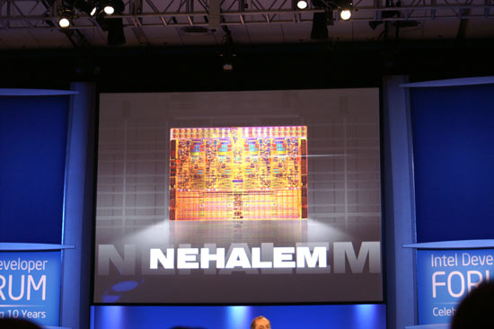
News in the last 24 hours, based on public statements, states that former Intel Senior Fellow Glenn Hinton, who lists being the lead architect of Intel’s Nehalem CPU core in his list of achievements, is coming out of retirement to re-join the company. (The other lead architect of Nehalem are Ronak Singhal and Per Hammerlund - Ronak is still at Intel, working on next-gen processors, while Per has been at Apple for five years.)
Hinton is an old Intel hand, with 35 years of experience, leading microarchitecture development of Pentium 4, one of three senior architects of Intel’s P6 processor design (which led to Pentium Pro, P2, P3), and ultimately one of the drivers to Intel’s Core architecture which is still at the forefront of Intel’s portfolio today. He also a lead microarchitect for Intel’s i960 CA, the world’s first super-scalar microprocessor. Hinton holds more than 90+ patents from 8 CPU designs from his endeavors. Hinton spent another 10+ years at Intel after Nehalem, but Nehalem is listed in many places as his primary public achievement at Intel.

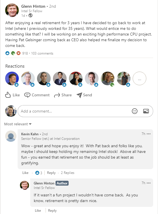
On his social media posts, Hinton states that he will be working on ‘an exciting high performance CPU project’. In the associated comments also states that ‘if it wasn’t a fun project I wouldn’t have come back – as you know, retirement is pretty darn nice’. Glenn also discloses that he has been pondering the move since November, and Gelsinger’s re-hiring helped finalize that decision. His peers also opine that Glenn is probably not the only ex-Intel architect that might be heading back to the company. We know a few architects and specialists that have left Intel in recent years to join Intel's competitors, such as AMD and Apple.
There are a few key things to note here worth considering.
First is that coming out of retirement for a big CPU project isn’t a trivial thing, especially for an Intel Senior Fellow. Given Intel’s successes, one would assume that the financial situation is not the main driver here, but the opportunity to work on something new and exciting. Plus, these sorts of projects take years of development, at least three, and thus Glenn is signing on for a long term despite already having left to retire.
Second point is reiterating that last line – whatever project Glenn is working on, it will be a long term project. Assuming that Glenn is talking about a fresh project within Intel’s R&D ecosystem, it will be 3-5 years before we see the fruits of the labor, which also means creating a design aimed at what could be a variety of process node technologies. Glenn’s expertise as lead architect is quite likely applicable for any stage of an Intel R&D design window, but is perhaps best served from the initial stages. The way Glenn seems to put it, this might be a black-ops style design. It also doesn't specify if this is x86, leaving that door open to speculation.
Third here is to recognize that Intel has a number of processor design teams in-house and despite the manufacturing process delays, they haven’t been idle. We’ve been seeing refresh after refresh of Skylake lead Intel's portfolio, and while the first iterations of the 10nm Cove cores come to market, Intel’s internal design teams would have been working on the next generation, and the next generation after that – the only barrier to deployment would have been manufacturing. I recall a discussion with Intel’s engineers around Kaby Lake time, when I asked about Intel’s progress on IPC – I requested a +10% gen-on-gen increase over the next two years at the time, and I was told that those designs were done and baked – they were already working on the ones beyond that. Those designs were likely Ice/Tiger Lake, and so Intel’s core design teams have been surging ahead despite manufacturing issues, and I wonder if there’s now a 3-4 year (or more) delay on some of these designs. If Glenn is hinting at a project beyond that, then we could be waiting even longer.
Fourth and finally, one of the critical elements listed by a number of analysts on the announcement of Gelsinger’s arrival was that he wouldn’t have much of an effect until 3+ years down the line, because of how product cycles work. I rejected that premise outright, stating that Pat can come in and change elements of Intel’s culture immediately, and could sit in the room with the relevant engineers and discuss product design on a level that Bob Swan cannot. Pat has the opportunity to arrange the leadership structure and instill new confidence in those structures, some of which may have caused key architects in the past to retire, instead of build on exciting projects.
As we can see, Pat is already having an effect before his name is even on the door at HQ.
Today is also Intel’s end-of-year financial disclosure, at 5pm ET. We are expecting Intel’s current CEO, Bob Swan, to talk through what looks to be another record breaking year of revenue, and likely the state of play for Intel's own 7nm process node technologies. That last point is somewhat thrown into doubt given the new CEO announcement and if Gelsinger is on the call. It is unknown if Gelsinger will participate.
Related Reading
- Intel Appoints Pat Gelsinger as New CEO, From Feb 15th
- An Interview with Intel CEO Bob Swan: Roundtable Q&A on Fabs and Future
- Robert Swan Named CEO of Intel


112 Comments
View All Comments
JayNor - Friday, January 22, 2021 - link
Intel has given their Client 2.0 presentation ... stitching and stacking chiplets. They also taped out a stacked SRAM, built with hybrid bonding last year. They also are introducing CXL into the server CPUs and GPUs this year. They also demoed co-packaged photonics last year. The also shipped their first foveros 3d chip design last year.All these seem to enable new paths for chip designs, including architectures.
I could see CPU cores turning into accelerators with large, biased private caches, for example, as being a natural extension of the CXL XPU designs that are being conceived for ai/hpc processing.
mode_13h - Saturday, January 23, 2021 - link
Neural network hardware is not intrinsically Von Neumann, though it can be implemented that way.I'm not familiar enough with graph analytics processors to say whether they potentially break Von Neumann, as well.
FPGAs are also not intrinsically Von Neumann, though can obviously be used that way.
And what do people think about transport-triggered architectures? Fundamentally asych computing strikes me as fairly non-Von Neumann.
For the sake of completeness, other non-Von Neumann architectures that come to mind are analog and quantum. Analog has some potential for neural computing. I think Intel's Ni1000 was analog?
Anyway, it's always hard for a new technology to usurp an old one. Just look at how long it took for NAND flash to overtake HDDs! You could see it coming for decades, but HDDs just kept improving fast enough to stay ahead of it for quite a while. In a similar way, Dennard scaling enabled Von Neumann architectures to evolve rapidly enough to keep from being overtaken, and software compatibility provided a big enough hurdle that nothing else was able to mount a serious threat. However, as manufacturing tech runs out of steam, perhaps the industry will finally be driven to revisit some of the more fringe computer architecture ideas that've been left by the wayside.
Lord of the Bored - Friday, January 22, 2021 - link
Because in this case the old hands are genuinely good at this. Microprocessor design is not a field where skills rapidly expire. Fresh blood, by contrast, has no proven track record and will likely have to spend time learning what works, from ... the old hands.Apple's CPU design team also eked out a good degree of their performance by making design compromises that wouldn't be acceptable in the x86 market.
Notably, system RAM is integrated into the CPU package. This greatly boosts performance, but also greatly limits capacity and completely negates upgradability. Intel knows about this, and started pulling cache into the processor with the 486, but they can't do the same for main memory. The x86 market wants their DIMM slots, wants to be able to take one CPU and pair it with arbitrary amounts of RAM(where arbitrary<256TB, anyways), so that is a major performance hack that is immediately off the table.
GeoffreyA - Friday, January 22, 2021 - link
According to infallible modern thinking, old is bad and new is good.FunBunny2 - Friday, January 22, 2021 - link
"Notably, system RAM is integrated into the CPU package."from an RDBMS point of view, likely any transaction, having a true 'single level store' makes ACID come out in the wash, and negates all other store methods. Optane is a step in that direction. this will require 'new' ways to manage transactions, in that currently RDBMS (as an example) will write to some log first (usually, but not necessarily) then to the database. whether such a two-step transactional protocol is still required for a memory-only storage? belt and suspenders?
mode_13h - Saturday, January 23, 2021 - link
> Notably, system RAM is integrated into the CPU package. This greatly boosts performance, but also greatly limits capacity and completely negates upgradability.Use HBM2 as L4 cache and 3D XPoint for expandability. Software can even treat the HBM2 as system RAM and swap to Optane DIMMs.
Rookierookie - Thursday, January 21, 2021 - link
I am excited to see that they are hiring the people who developed Pentium 4.DigitalFreak - Thursday, January 21, 2021 - link
Yeah, I was going to say 'leading microarchitecture development of Pentium 4' isn't something to be proud of.The Hardcard - Thursday, January 21, 2021 - link
Why would team membersnot be proud of the Pentium 4, or Bulldozer for that matter?Those failures were not because of incompetent designers and engineers who just didn’t know what they were doing. They were simply bets that were made at the company level. The staff to be done with a finite amount of resources, a finite amount of money, a finite amount of time, and particular product targets - all if which affect cgances of success.
Nearly every designer and all of those teams could also work on other teams. Not that there aren’t some who are better than others, but they all can work on successful architectures. Just as they can all work on failures, and probably have.
Pentium 4 and Bulldozer required just as much intelligence, imagination, and work ethic as the M1. In the quest for technical leadership, bets like these have to be made. There are no guarantees when you go in.
lmcd - Thursday, January 21, 2021 - link
Bulldozer was a bet that GCN would both reach maturity sooner, and be flexible enough to realistically take over floating point compute, while said GCN products had no good compute API (no, OpenCL does not count as "good").That's a company failure for sure. It was also a manufacturing failure -- people act like Intel's struggles in manufacturing are unique to it, but AMD was stuck at 32nm/28nm for about as long as Intel has been stuck at 14nm.
P4 micro-op cache was revolutionary, but not yet ready for prime time. Also it was Intel's first SMT architecture! I'd argue the features Intel developed for P4 were essential, but hindered by the mistake of a long pipeline and less-accurate branch prediction.