Using a PCIe Slot to Install DRAM: New Samsung CXL.mem Expansion Module
by Dr. Ian Cutress on May 11, 2021 4:10 AM EST- Posted in
- Interconnect
- Samsung
- DRAM
- DDR5
- Compute Express Link
- CXL
- PCIe 5.0
- CXL.memory
In the computing industry, we’ve lived with PCIe as a standard for a long time. It is used to add any additional features to a system: graphics, storage, USB ports, more storage, networking, add-in cards, storage, sound cards, Wi-Fi, oh did I mention storage? Well the one thing that we haven’t been able to put into a PCIe slot is DRAM – I don’t mean DRAM as a storage device, but memory that actually is added to the system as useable DRAM. Back in 2019 a new CXL standard was introduced, which uses a PCIe 5.0 link as the physical interface. Part of that standard is CXL.memory – the ability to add DRAM into a system through a CXL/PCIe slot. Today Samsung is unveiling the first DRAM module specifically designed in this way.
CXL: A Refresher
The original CXL standard started off as a research project inside Intel to create an interface that can support accelerators, IO, cache, and memory. It subsequently spun out into its own consortium, with over 50+ members, and support from key players in the industry: Intel, AMD, Arm, IBM, Broadcom, Marvell, NVIDIA, Samsung, SK Hynix, WD, and others. The latest standard is CXL 2.0, finalized in November 2020.
The CXL 1.1 standard covers three sets of intrinsics, known as CXL.io, CXL.memory and CXL.cache. These allow for deeper control over the connected devices, as well as an expansion as to what is possible. The CXL consortium sees three main areas for this:

The first type is a cache/accelerator, such as an offload engine or a SmartNIC (a smart network controller). With the CXL.io and CXL.cache intrinsics, this would allow the network controller to sort incoming data, analyze it, and filter what is needed directly into the main processors memory.
The second type is an accelerator with memory, and direct access to the HBM on the accelerator from the processor (as well as access to DRAM from the accelerator). The idea is a pseudo-heterogeneous compute design allowing for simpler but dense computational solvers.
The third type is perhaps the one we’re most interested in today: memory buffers. Using CXL.memory, a memory buffer can be installed over a CXL link and the attached memory can be directly pooled with the system memory. This allows for either increased memory bandwidth, or increased memory expansion, to the order of thousands of gigabytes.
CXL 2.0 also introduces CXL.security, support for persistent memory, and switching capabilities.
It should be noted that CXL is using the same electrical interface as PCIe. That means any CXL device will have what looks like a PCIe physical connector. Beyond that, CXL uses PCIe in its startup process, so currently any CXL supporting device has to also support a PCIe-to-PCIe link, making any CXL controller also a PCIe controller by default.
One of the common questions I’ve seen is what would happen if a CXL-only CPU was made? Because CXL and PCIe are intertwined, a CPU can’t be CXL-only, it would have to support PCIe connections as well. That being said, from the other direction: if we see CXL-based graphics cards for example, they would also have to at least initialize over PCIe, however full working modes might not be possible if CXL isn’t initialized.
Intel is set to introduce CXL 1.1 over PCIe 5.0 with its Sapphire Rapids processors. Microchip has announced PCIe 5.0 and CXL-based retimers for motherboard trace extensions. Samsung today is the third announcement for CXL supported devices. IBM has a similar technology called OMI (OpenCAPI Memory Interface), however that hasn’t seen wide adoption outside of IBM’s own processors.
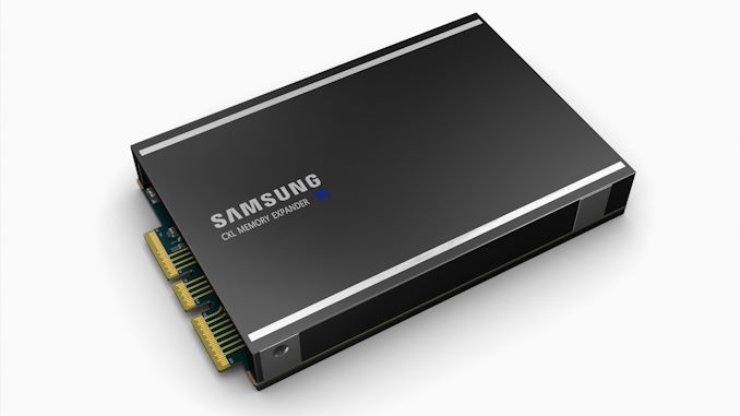
Samsung’s CXL Memory Module
Modern processors rely on memory controllers for attached DRAM access. The top line x86 processors have eight channels of DDR4, while a number of accelerators have gone down the HBM route. One of the limiting factors in scaling up memory bandwidth is the number of controllers, which can also limit capacity, and beyond that memory needs to be validated and trained to work with a system. Most systems are not built to simply add or remove memory the same way you might do with a storage device.
Enter CXL, and the ability to add memory like a storage device. Samsung’s unveiling today is of a CXL-attached module packed to the max with DDR5. It uses a full PCIe 5.0 x16 link, allowing for a theoretical bidirectional 32 GT/s, but with multiple TB of memory behind a buffer controller. In much the same way that companies like Samsung pack NAND into a U.2-sized form factor, with sufficient cooling, Samsung does the same here but with DRAM.
The DRAM is still a volatile memory, and data is lost if power is lost. (I doubt it is hot swappable either, but weirder things have happened). Persistent memory can be used, but only with CXL 2.0. Samsung hasn't stated if their device supports CXL 2.0, but it should be at least CXL 1.1 as they state it currently is being tested with Intel's Sapphire Rapids platform.
It should be noted that a modern DRAM slot is usually rated maximum for ~18W. The only modules in that power window are Intel’s Optane DCPMM, but a 256 GB DDR4 module would be in that ~10+ W range. For a 2 TB add-in CXL module like this, I suspect we are looking at around 70-80 W, and so to add that amount of DRAM through the CXL interface would likely require active cooling as well as the big heatsink that these renders suggest.
Samsung doesn’t give any details about the module they are unveiling, except that it is CXL based and has DDR5 in it. Not only that, but the ‘photos’ provided look a lot like renders, so it’s hard to state if they have an aesthetic unit available for photography, or if there’s simply a working controller in a bring-up lab somewhere that has been validated on a system. Update: Samsung has confirmed these are live shots, not renders.
As part of the announcement Samsung quoted AMD and Intel, indicating which partners they are more closely working with, and what they have today is being validated on Intel next-gen servers. Intel’s next-gen servers, Sapphire Rapids, are due to launch at the end of the year, in line with the Aurora supercomputing contract set to be initially shipped by year end.
Related Reading
- Compute eXpress Link 2.0 (CXL 2.0) Finalized: Switching, PMEM, Security
- CXL Consortium Formally Incorporated, Gets New Board Members & CXL 1.1 Specification
- CXL Specification 1.0 Released: New Industry High-Speed Interconnect From Intel
- Intel Agilex: 10nm FPGAs with PCIe 5.0, DDR5, and CXL
- Synopsys Demonstrates CXL and CCIX 1.1 over PCIe 5.0: Next-Gen In Action
- Microchip Announces PCIe 5.0 And CXL Retimers
- DDR5 Memory Specification Released: Setting the Stage for DDR5-6400 And Beyond
- Here's Some DDR5-4800: Hands-On First Look at Next Gen DRAM
- Insights into DDR5 Sub-timings and Latencies


47 Comments
View All Comments
schujj07 - Thursday, May 13, 2021 - link
32GT/s =/ 256GB/sec. Each lane does 32GT (32Gbit) * 16 lanes = 512GT/s (512Gbit) / 8 (8 bits per byte) = 64GB/sec.That is roughly the throughput of dual channel DDR4-4000 just with more overhead and longer connections. Realistically figure that number would drop by 10-20% over theoretical maximum.mode_13h - Thursday, May 13, 2021 - link
That's per-direction, FWIW. So, depending on the CXL protocol and their implementation, it's conceivable you could hit 2x that, if your reads and writes are somewhat balanced.I agree with your approach, however. Since there are so many caveats around bi-dir throughput, we should just focus on the uni-dir numbers and hope bi-dir is higher.
schujj07 - Friday, May 14, 2021 - link
When talking about bandwidth, you never state a 64GB/sec bi-directional link is a 128GB/sec connection. The stated bandwidth is always said in the uni-directional numbers, however, you might say it is 64GB/sec bi-directional.Exotica - Tuesday, May 11, 2021 - link
When PCI 6.0 drops, this will have even more bandwidth abilities. And with cxl 2.0, Persistent memory could be coming to the mainstream.Tomatotech - Tuesday, May 11, 2021 - link
A weird wafer-munching wizard wrote about CXL 2.0 over here:https://www.anandtech.com/show/16227/compute-expre...
DanNeely - Tuesday, May 11, 2021 - link
Well this is a blast from the past. Back in the 80s you could add more ram to your PC over the ISA bus. exhttps://www.lo-tech.co.uk/wiki/Lo-tech_1MB_RAM_Boa...
Lucky Stripes 99 - Tuesday, May 11, 2021 - link
Same with your Commodore Amiga and a Zorro bus card. Some were even combo cards that also included a SCSI controller and a space to mount a 3.5" hard drive (a so-called "hard card").When I bought an M.2 NVMe PCIe expansion card a couple years ago, I had a bit of a "what's old is new again" feeling from my old computer days.
watersb - Wednesday, May 12, 2021 - link
The new DRAM modules could be called "QuadRam"... It has a nice ring to it...abufrejoval - Tuesday, May 11, 2021 - link
Just reminds me how normal it used to be to have RAM in extra boards.S100 systems always used separate memory boards, Apple ][ gave you an extra 16KB with the language card and my 1.5MB Intel Above board came with an 80287 and Windows 1.0 as goodies ("who would ever need more than 640k in a PC?").
Never really noticed when they stopped putting RAM into add-on cards but noted how HPC code has spent decades trying to hide where the memory actually is. With the number of memory tiers constantly increasing, CXL will help some code adapting itself to take advantage of potential gains, but I don't envy those who have to write and validate the code that makes it happen.
Duncan Macdonald - Tuesday, May 11, 2021 - link
High bandwidth may be possible but what is the latency ? How long will it take a CPU to read a location in one of these modules vs reading a location in directly attached memory.From the various CPU tests that have been done here - ordinary random RAM access is in the order of 80ns - how much overhead will the CXL/PCIe interface and protocols add ?