Did IBM Just Preview The Future of Caches?
by Dr. Ian Cutress on September 2, 2021 9:00 AM EST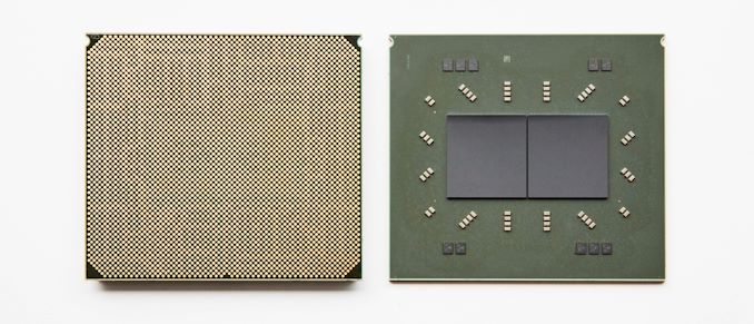
At Hot Chips last week, IBM announced its new mainframe Z processor. It’s a big interesting piece of kit that I want to do a wider piece on at some point, but there was one feature of that core design that I want to pluck out and focus on specifically. IBM Z is known for having big L3 caches, backed with a separate global L4 cache chip that operates as a cache between multiple sockets of processors – with the new Telum chip, IBM has done away with that – there’s no L4, but interestingly enough, there’s no L3. What they’ve done instead might be an indication of the future of on-chip cache design.
Caches: A Brief Primer
Any modern processor has multiple levels of cache associated with it. These are separated by capacity, latency, and power – the fastest cache closest to the execution ports tends to be small, and then further out we have larger caches that are slightly slower, and then perhaps another cache before we hit main memory. Caches exist because the CPU core wants data NOW, and if it was all held in DRAM it would take 300+ cycles each time to fetch data.
A modern CPU core will predict what data it needs in advance, bring it from DRAM into its caches, and then the core can grab it a lot faster when it needs it. Once the cache line is used, it is often ‘evicted’ from the closest level cache (L1) to the next level up (L2), or if that L2 cache is full, the oldest cache line in the L2 will be evicted to an L3 cache to make room. It means that if that data line is ever needed again, it isn’t too far away.
An example of L1, L2, and a shared L3 on AMD's First Gen Zen processors
There is also the scope of private and shared caches. A modern processor design has multiple cores, and inside those cores will be at least one private cache (the L1) that only that core has access to. Above that, a cache may either be a private cache still local to the core, or a shared cache, which any core can use. An Intel Coffee Lake processor for example has eight cores, and each core has a 256 KB private L2 cache, but chip wide there is a 16 MB shared L3 between all eight cores. This means that if a single core wants to, it can keep evicting data from its smaller L2 into the large L3 and have a pool of resources if that data wants to be reused. Not only this, but if a second core needs some of that data as well, they can find it in the shared L3 cache without having to write it out to main memory and grab it there. To complicate the matter, a 'shared' cache isn't necessarily shared between all cores, it might only be shared between a specific few.
The end result is that caches help reduce time to execution, and bring in more data from main memory in case it is needed or as it is needed.
Tradeoffs
With that in mind, you might ask why we don’t see 1 GB L1 or L2 caches on a processor. It’s a perfectly valid question. There are a number of elements at play here, involving die area, utility, and latency.
The die area is an easy one to tackle first – ultimately there may only be a defined space for each cache structure. When you design a core in silicon, there may be a best way to lay the components of the core out to have the fastest critical path. But the cache, especially the L1 cache, has to be close to where the data is needed. Designing that layout with a 4 KB L1 cache in mind is going to be very different if you want a large 128 KB L1 cache instead. So there is a tradeoff there – beyond the L1, the L2 cache is sometimes a large consumer of die space, and while it (usually) isn’t as constrained by the rest of the core design, it still has to be balanced with what is needed on the chip. Any large shared cache, whether it ends up as a level 2 cache or a level 3 cache, can often be the biggest part of the chip, depending on the process node used. Sometimes we only focus on the density of the logic transistors in the core, but with super large caches, perhaps the cache density is more important in what process node ends up being used.
Utility is also a key factor – we mostly speak about general purpose processors here on AnandTech, especially those built on x86 for PCs and servers, or Arm for smartphones and servers, but there are lots of dedicated designs out there whose role is for a specific workload or task. If all a processor core needs to do is process data, for example a camera AI engine, then that workload is a well-defined problem. That means the workload can be modelled, and the size of the caches can be optimized to give the best performance/power. If the purpose of the cache is to bring data close to the core, then any time the data isn’t ready in the cache, it’s called a cache miss – the goal of any CPU design is to minimize cache misses in exchange for performance or power, and so with a well-defined workload, the core can be built around the caches needed for an optimum performance/cache miss ratio.
Latency is also a large factor in how big caches are designed. The more cache you have, the longer it takes to access – not only because of the physical size (and distance away from the core), but because there’s more of it to search through. For example, small modern L1 caches can be accessed in as little as three cycles, whereas large modern L1 caches may be five cycles of latency. A small L2 cache can be as low as eight cycles, whereas a large L2 cache might be 19 cycles. There’s a lot more that goes into cache design than simply bigger equals slower, and all of the big CPU design companies will painstakingly work to shave those cycles down as much as possible, because often a latency saving in an L1 cache or an L2 cache offers good performance gains. But ultimately if you go bigger, you have to cater for the fact that the latency will often be larger, but your cache miss rate will be lower. This comes back to the previous paragraph talking about defined workloads. We see companies like AMD, Intel, Arm and others doing extensive workload analysis with their big customers to see what works best and how their core design should develop.
So What Has IBM Done That is So Revolutionary?
In the first paragraph, I mentioned that IBM Z is their big mainframe product – this is the big iron of the industry. It’s built better than your government-authorized nuclear bunker. These systems underpin the critical elements of society, such as infrastructure and banking. Downtime of these systems is measured in milliseconds per year, and they have fail safes and fail overs galore – with a financial transaction, when it is made, it has to be committed to all the right databases without fail, or even in the event of physical failure along the chain.
This is where IBM Z comes in. It’s incredibly niche, but has incredibly amazing design.
In the previous generation z15 product, there was no concept of a 1 CPU = 1 system product. The base unit of IBM Z was a five processor system, using two different types of processor. Four Compute Processors (CP) each housed 12 cores and 256 MB of shared L3 cache in 696mm2 built on 14nm running at 5.2 GHz. These four processors split into two pairs, but both pairs were also connected to a System Controller (SC), also 696mm2 and on 14nm, but this system controller held 960 MB of shared L4 cache, for data between all four processors.
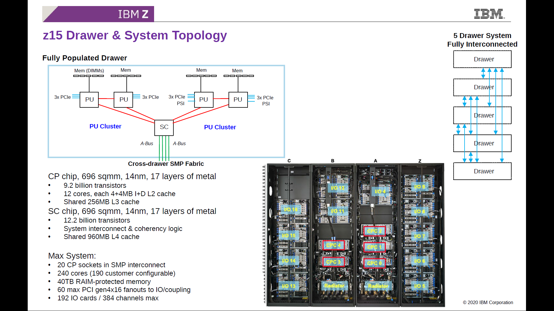
Note that this system did not have a ‘global’ DRAM, and each Compute Processor had its own DDR backed equivalent memory. IBM would then combine this five processor ‘drawer’, with four others for a single system. That means a single IBM z15 system was 25 x 696mm2 of silicon, 20 x 256 MB of L3 cache between them, but also 5 x 960 MB of L4 cache, connected in an all-to-all topology.
IBM z15 is a beast. But the next generation IBM Z, called IBM Telum rather than IBM z16, takes a different approach to all that cache.
IBM, Tell’em What To Do With Cache
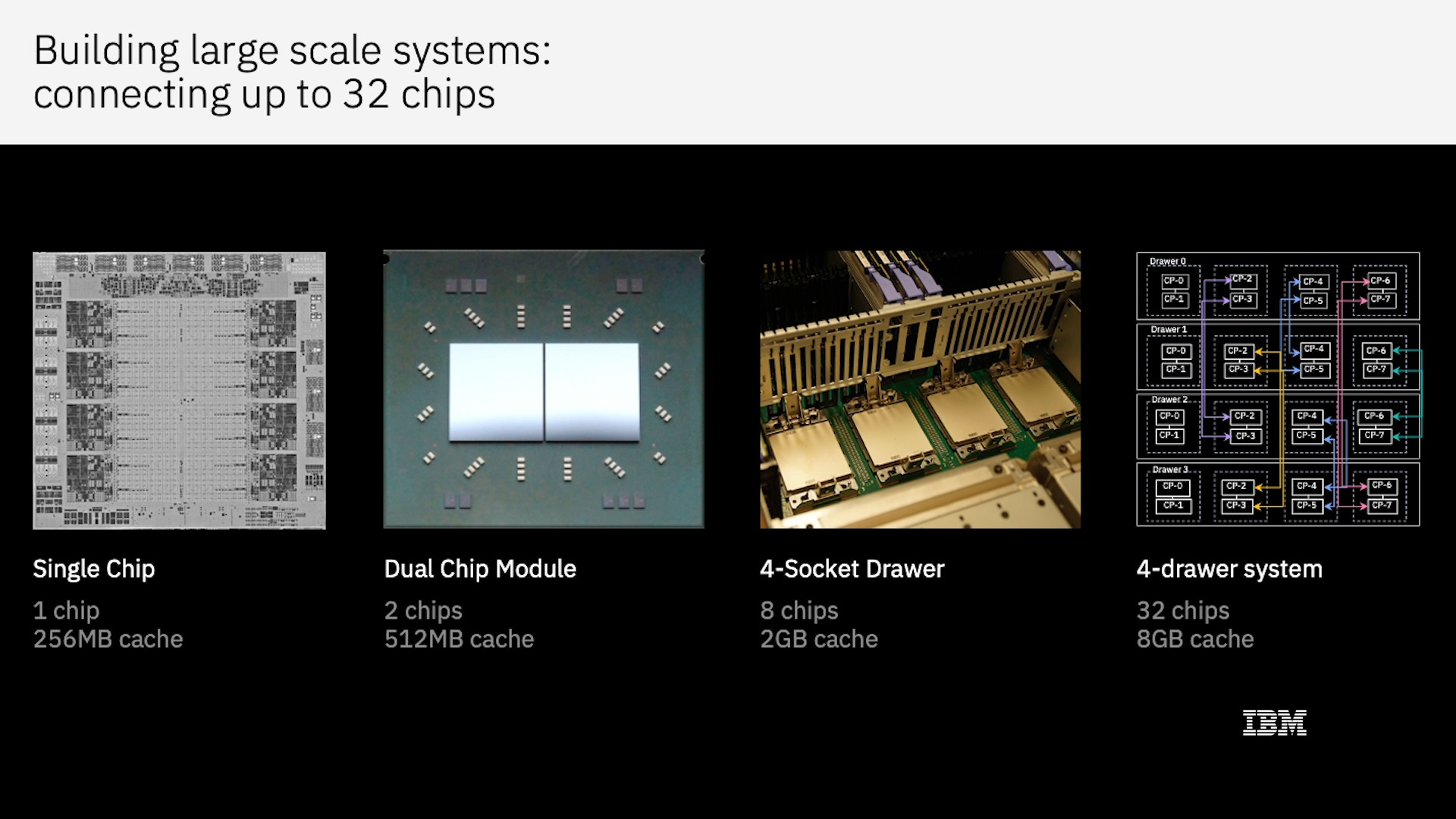
The new system does away with the separate System Controller with the L4 cache. Instead we have what looks like a normal processor with eight cores. Built on Samsung 7nm and at 530mm2, IBM packages two processors together into one, and then puts four packages (eight CPUs, 64 cores) into a single unit. Four units make a system, for a total of 32 CPUs / 256 cores.
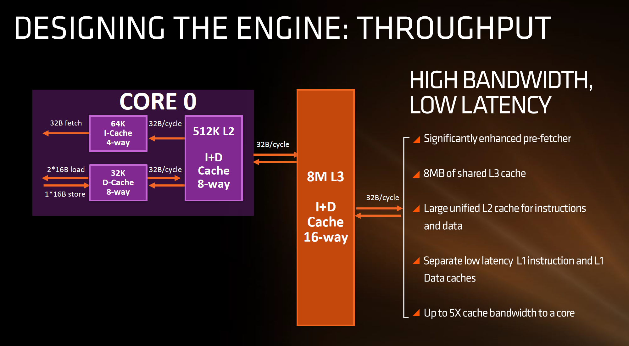
On a single chip, we have eight cores. Each core has 32 MB of private L2 cache, which has a 19-cycle access latency. This is a long latency for an L2 cache, but it’s also 64x bigger than Zen 3's L2 cache, which is a 12-cycle latency.

Looking at the chip design, all that space in the middle is L2 cache. There is no L3 cache. No physical shared L3 for all cores to access. Without a centralized cache chip as with z15, this would mean that in order for code that has some amount of shared data to work, it would need a round trip out to main memory, which is slow. But IBM has thought of this.
The concept is that the L2 cache isn’t just an L2 cache. On the face of it, each L2 cache is indeed a private cache for each core, and 32 MB is stonkingly huge. But when it comes time for a cache line to be evicted from L2, either purposefully by the processor or due to needing to make room, rather than simply disappearing it tries to find space somewhere else on the chip. If it finds a space in a different core’s L2, it sits there, and gets tagged as an L3 cache line.
What IBM has implemented here is the concept of shared virtual caches that exist inside private physical caches. That means the L2 cache and the L3 cache become the same physical thing, and that the cache can contain a mix of L2 and L3 cache lines as needed from all the different cores depending on the workload. This becomes important for cloud services (yes, IBM offers IBM Z in its cloud) where tenants do not need a full CPU, or for workloads that don’t scale exactly across cores.
This means that the whole chip, with eight private 32 MB L2 caches, could also be considered as having a 256 MB shared ‘virtual’ L3 cache. In this instance, consider the equivalent for the consumer space: AMD’s Zen 3 chiplet has eight cores and 32 MB of L3 cache, and only 512 KB of private L2 cache per core. If it implemented a bigger L2/virtual L3 scheme like IBM, we would end up with 4.5 MB of private L2 cache per core, or 36 MB of shared virtual L3 per chiplet.
This IBM Z scheme has the lucky advantage that if a core just happens to need data that sits in virtual L3, and that virtual L3 line just happens to be in its private L2, then the latency of 19 cycles is much lower than what a shared physical L3 cache would be (~35-55 cycle). However what is more likely is that the virtual L3 cache line needed is in the L2 cache of a different core, which IBM says incurs an average 12 nanosecond latency across its dual direction ring interconnect, which has a 320 GB/s bandwidth. 12 nanoseconds at 5.2 GHz is ~62 cycles, which is going to be slower than a physical L3 cache, but the larger L2 should mean less pressure on L3 use. But also because the size of L2 and L3 is so flexible and large, depending on the workload, overall latency should be lower and workload scope increased.
But it doesn’t stop there. We have to go deeper.
For IBM Telum, we have two chips in a package, four packages in a unit, four units in a system, for a total of 32 chips and 256 cores. Rather than having that external L4 cache chip, IBM is going a stage further and enabling that each private L2 cache can also house the equivalent of a virtual L4.
This means that if a cache line is evicted from the virtual L3 on one chip, it will go find another chip in the system to live on, and be marked as a virtual L4 cache line.
This means that from a singular core perspective, in a 256 core system, it has access to:
- 32 MB of private L2 cache (19-cycle latency)
- 256 MB of on-chip shared virtual L3 cache (+12ns latency)
- 8192 MB / 8 GB of off-chip shared virtual L4 cache (+? latency)
Technically from a single core perspective those numbers should probably be 32 MB / 224 MB / 7936 MB because a single core isn’t going to evict an L2 line into its own L2 and label it as L3, and so on.
IBM states that using this virtual cache system, there is the equivalent of 1.5x more cache per core than the IBM z15, but also improved average latencies for data access. Overall IBM claims a per-socket performance improvement of >40%. Other benchmarks are not available at this time.
How Is This Possible?
Magic. Honestly, the first time I saw this I was a bit astounded as to what was actually going on.
In the Q&A following the session, Dr. Christian Jacobi (Chief Architect of Z) said that the system is designed to keep track of data on a cache miss, uses broadcasts, and memory state bits are tracked for broadcasts to external chips. These go across the whole system, and when data arrives it makes sure it can be used and confirms that all other copies are invalidated before working on the data. In the slack channel as part of the event, he also stated that lots of cycle counting goes on!
I’m going to stick with magic.
Truth be told, a lot of work goes into something like this, and there’s likely still a lot of considerations to put forward to IBM about its operation, such as active power, or if caches be powered down in idle or even be excluded from accepting evictions altogether to guarantee performance consistency of a single core. It makes me think what might be relevant and possible in x86 land, or even with consumer devices.
I’d be remiss in talking caches if I didn’t mention AMD’s upcoming V-cache technology, which is set to enable 96 MB of L3 cache per chiplet rather than 32 MB by adding a vertically stacked 64 MB L3 chiplet on top. But what would it mean to performance if that chiplet wasn’t L3, but considered an extra 8 MB of L2 per core instead, with the ability to accept virtual L3 cache lines?
Ultimately I spoke with some industry peers about IBM’s virtual caching idea, with comments ranging from ‘it shouldn’t work well’ to ‘it’s complex’ and ‘if they can do it as stated, that’s kinda cool’.


149 Comments
View All Comments
LightningNZ - Sunday, September 5, 2021 - link
> Why? If the cache is dealing in physical addresses and the OS is ensuring that no two virtual addresses overlap (or, any thing do have explicit its approval), then why would the cache also need to know the virtual address?You're right. As long as you stored the entire 64-bits of the address it shouldn't be an issue. That would boost its density too
LightningNZ - Monday, September 6, 2021 - link
I forgot in my first reply that if you don't have virtual tagging then you can't tell a core making a request where the data may be above it - that information could be currently in another cache. You'd have to have resolved probes and whatever already, so it's not just another level in the cache hierarchy, but a dumb latency reducer for DRAM accesses. It'd have to be quite large to be much use I'd have thought to give much benefit if you'd already traversed all other caches.ZolaIII - Friday, September 3, 2021 - link
They have my applause on L2 size but other than that it's a victim of/to victim, if they went with a much larger memory cube (HMC) and interesting buss (which would still be in the same role) I would have said fine. Would really like to see consumer grade (mobile/tablet/laptop...) SoC's where it can serve (either cube or HBM) as final RAM (as neither the DDR latency nor new buffer levels have much sense anymore).misan - Friday, September 3, 2021 - link
Isn’t Apple already doing something like that with their shared L2 cache? From benchmarks done by Anandtech it seems like every M1 core has „priority“ access to a portion of L2 and the rest is used as some sort of a virtual L3.AntonErtl - Friday, September 3, 2021 - link
Unfortunately, the article just reaffirmed what I understood from the little bit that the slides shown at HotChips revealed already. The interesting pieces are missing: When is a line in a different L2 considered "unused"? How does that information get communicated? Is the system using directories, or is it just snooping?Some ideas that come to my mind is a directory at each memory controller that tells which lines for this memory controller are in which cache(s); this would keep traffic down, but may increase latency.
Brane2 - Friday, September 3, 2021 - link
Another bunch of marketing nonsense.I'm sure IBM chose the model that fits THEIR use patterns the best.
Which is usually far from what others in x86_64 land might see.
What is interesting is how easily have they managed to sell it to "doctor" Ian Cutress...
Doctor of what ?
19 cycles is not that great for L2. Above that, 12ns is not that great for on-the-chip communication.
Above that, this L3/L4 from many L2 tiles doesn't seem to bring anything significant on inter-chip levels. Latencies are so big anyway that couple of cycles more or less don't mean much.
Also, L1,L2 and L3 are different beasts. One can't compare and translate their logic 1:1.
Oxford Guy - Friday, September 3, 2021 - link
You should read the article.Ian Cutress - Saturday, September 4, 2021 - link
Love your use of quotes.The answer to your question is simply 'heresy'. I studied and wrote a thesis on the mystic arts. I can identify magic when I see it.
mode_13h - Saturday, September 4, 2021 - link
Not sure exactly what's your issue. However, on the semantic front, those who distain use of the title "doctor" for Ph.D. recipients would do well to note that the distinction pre-dated Medical Doctorates by at least 5 centuries.FunBunny2 - Saturday, September 4, 2021 - link
"distinction pre-dated Medical Doctorates by at least 5 centuries."it wasn't until well into the 20th century that an MD actually had to attend a Medical School; it was not much more, if that, than an apprenticeship in blacksmithing.