Google's Tensor inside of Pixel 6, Pixel 6 Pro: A Look into Performance & Efficiency
by Andrei Frumusanu on November 2, 2021 8:00 AM EST- Posted in
- Mobile
- Smartphones
- SoCs
- Pixel 6
- Pixel 6 Pro
- Google Tensor
Memory Subsystem & Latency
Usually, the first concern of a SoC design, is that it requires that it performs well in terms of its data fabric and properly giving its IP blocks access to the caches and DRAM of the system within good latency metrics, as latency, especially on the CPU side, is directly proportional to the end-result performance under many workloads.
The Google Tensor, is both similar, but different to the Exynos chips in this regard. Google does however fundamentally change how the internal fabric of the chip is set up in terms of various buses and interconnects, so we do expect some differences.
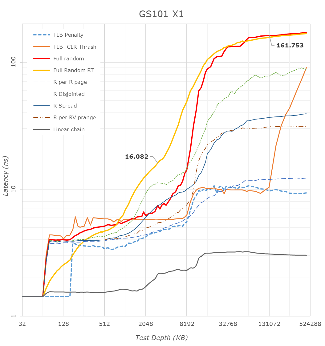
First off, we have to mention that many of the latency patterns here are still quite a broken due to the new Arm temporal prefetchers that were introduced with the Cortex-X1 and A78 series CPUs – please just pay attention to the orange “Full Random RT” curve which bypasses these.
There’s a couple of things to see here, let’s start at the CPU side, where we see the X1 cores of the Tensor chip being configured with 1MB of L2, which comes in contrast with the smaller 512KB of the Exynos 2100, but in line with what we see on the Snapdragon 888.
The second thing to note, is that it looks like the Tensor’s DRAM latency isn’t good, and showcases a considerable regression compared to the Exynos 2100, which in turn was quite worse off than the Snapdragon 888. While the measurements are correct in what they’re measuring, the problem is a bit more complex in the way that Google is operating the memory controllers on the Google Tensor. For the CPUs, Google is tying the MCs and DRAM speed based on performance counters of the CPUs and the actual workload IPC as well as memory stall % of the cores, which is different to the way Samsung runs things which are more transactional utilisation rate of the memory controllers. I’m not sure of the high memory latency figures of the CPUs are caused by this, or rather by simply having a higher latency fabric within the SoC as I wasn’t able to confirm the runtime operational frequencies of the memory during the tests on this unrooted device. However, it’s a topic which we’ll see brought up a few more times in the next few pages, especially on the CPU performance evaluation of things.
The Cortex-A76 view of things looks more normal in terms of latencies as things don’t get impacted by the temporal prefetchers, still, the latencies here are significantly higher than on competitor SoCs, on all patterns.
What I found weird, was that the L3 latencies of the Tensor SoC also look to be quite high, above that of the Exynos 2100 and Snapdragon 888 by quite a noticeable margin. I noted that one weird thing about the Tensor SoC, is that Google didn’t give the DSU and the L3 cache of the CPU cluster a dedicated clock plane, rather tying it to the frequency of the Cortex-A55 cores. The odd thing here is that, even if the X1 or A76 cores are under full load, the A55 cores as well as the L3 are still running at lower frequencies. The same scenario on the Exynos or Snapdragon chip would raise the frequency of the L3. This behaviour and aspect of the chip can be confirmed by running at dummy load on the Cortex-A55 cores in order to drive the L3 higher, which improves the figures on both the X1 and A76 cores.
The system level cache is visible in the latency hump starting at around 11-13MB (1MB L2 + 4MB L3 + 8MB SLC). I’m not showing it in the graphs here, but memory bandwidth on normal accesses on the Google chip is also slower than on the Exynos, but I think I do see more fabric bandwidth when doing things such as modifying individual cache lines – one of the reasons I think the SLC architecture is different than what’s on the Exynos 2100.
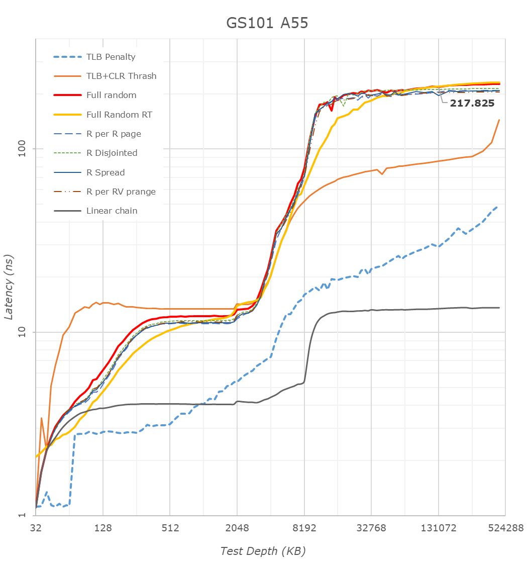
The A55 cores on the Google Tensor have 128KB of L2 cache. What’s interesting here is that because the L3 is on the same clock plane as the Cortex-A55 cores, and it runs at the same higher frequencies, is that the Tensor’s A55s have the lowest L3 latencies of the all the SoCs, as they do without an asynchronous clock bridge between the blocks. Like on the Exynos, there’s some sort of increase at 2MB, something we don’t see on the Snapdragon 888, and I think is related to how the L3 is implemented on the chips.
Overall, the Tensor SoC is quite different here in how it’s operated, and there’s some key behaviours that we’ll have to keep in mind for the performance evaluation part.


108 Comments
View All Comments
sharath.naik - Thursday, November 4, 2021 - link
Good in-depth review. I know you are doing the camera review of this. So I have a request can you look into if the Pixel 6 cameras are hardware binned to ~12MP even though the specs say they are 50MP/48MP. There is a lot of mixed views out there, most mistaking this as the pixel binning done on other phones like galaxy S21u(Software binned for low light but has access to full resolution). If you could confirm this for the review would be great, looking forward to that review.Silver5urfer - Tuesday, November 2, 2021 - link
Exactly as expected 1:1The SoC is a bust, they tried to do some gimmickry with their zero talent and tried to make it a cheaper deal by going to Samsung for their IP fabrication expertise and lithography process. Ended up being a dud in CPU, GPU and price to performance, all that NPU NN, mega magic boom is all a farce. I was asking the same thing, what does these provide to us end users ? Nothing. Just that fancy Livetranslation and other gimmicks which you use seldom. On top we do not even know what TPU does in the Pixel Software, it's closed source. AOSP is open but Pixel UI and all backend are closed.
Hardware is utter joke, the P6 series has garbage mmwave system look at the internals, they crammed one lol. LG V50 back in 2019 had 2-33 mmwave antennas. This junk saved on cost. The display has banding issues all over the place. Optical image sensor for Fingerprint is slow and a joke vs the physical dedicated ones. The stereo speaker system has massive channel imbalance on top. Then you have the low battery SoT for this price point and battery capacity. The DIY aspect is thrown into gutters, the phone has massively hamfisted cooling approach with graphite pads smeared all over the place as leaks showed and no proper HS system it's just a small pathetic AL board reinforcement plate doing it so on top the Display has no metal backplate to reinforce it or dissipate heat. What a nonsense. SD888 itself heats up a lot and so many vendors add VC cooling, Sony Xperia 1 Mark 3 messed up there and had inferior performance with throttling. This junk is even more pathetic, pay for a S tier SKU get trash sustained performance of a B+ device, the AP, Pocket now and other Youtube shill press will hype this to moon.
We do not even know how this junk has in terms of Software blocks like P2, P3, P4 had A/B system, then merged partitions, later read only ext4 system. This will have even worse. To make it a round about trash, the software is a joke cheap kiddo inspired garbage, heck that BBKs OnePlus's Oxygen + Oppo Color OS mix is way superior than this junk with massive information density loss.
I'd wait for the next SD successor device, hopefully 888's BS power consumption and insane heat can be reduced.
Silver5urfer - Tuesday, November 2, 2021 - link
It's a typo for mmwave, it's 2-3 units. Also I forgot to mention the lack of charger, SD slot, no 3.5mm jack very poor servicing almost impossible to get the phone properly cooled if you open it due to cheap graphite pad reliance. It also has that USB port and microphone soldered to the mainboard which looks like a feeble trash unit check any phone in the recent times and look how solid engineered they are, dual sandwich designs with reinforced chassis and proper heat dissipation.goatfajitas - Tuesday, November 2, 2021 - link
People get WAY too hung up on benchmarks. LOL, a "dud". A phone is about user experience, not how many "geekmarks" = best.lionking80 - Tuesday, November 2, 2021 - link
I agree that the benchmarks do not tell the whole story, but I would still say that even the use of a Snapdragon 870 would have been a better choice.The general performance is similar (maybe a small advantage for Tensor in AI), but the advantages of Snapdragon 870 are bigger: runs much cooler, hugely better battery-life.
To be honest I am disappointed by the SOC. The only thing that might make it a seller is the software (ui and camera), but the SOC is rather a no-go.
goatfajitas - Tuesday, November 2, 2021 - link
There are other factors though. Early ROM settings, tweaks, bugs, and cooling/hardware. The 870 may have scored lower in a P6 as well. So many factors. - Agreed, the P6 should be a bit more polished though.at_clucks - Tuesday, November 2, 2021 - link
The problem goes beyond the slightly worse SoC than the already existing Qualcomm offering. It's that despite being a "Google SoC" they still support it for just 3 years. All the excuses used over the years, all the pointing fingers at SoC manufacturers for the lack of support were just proven to be a load of crap. Same crap, now with a google sticker.sharath.naik - Tuesday, November 2, 2021 - link
It's about to get worse with the camera review. I can verify Google might have been bluffing about the 50mp/48mp sensors. The sensors are locked at 12mp. So Pixel pro has essentially three 12 mp cameras. Which means the portrait mode zoom of 2x is a low resolution 3 MP image. Also at 10x zoom the image resolution is 2.5MP, 4 times lower than that of s21 ultra. What drove Google to make the choice of first hardware pixel binning the resolution down and then trying to digitally blow the resolution backup!!.It's baffling, tried to get an answer from Google support, they just refused to confirm or deny this is binned at the hardware levelhoxha_red - Tuesday, November 2, 2021 - link
"I can verify that google might have been bluffing"dude, lmfao—it's called "binning"; please look it up. they've been upfront about this and it was known before the phone was even launched, let alone after we've seen all of these reviews. The reason Google support "refused to confirm or deny" is because the people doing customer support are unlikely to know what "pixel binning" is (hey, I guess they're in good company there with you), and are not equipped to deal with weirdos of your specific variety.
Maxpower27 - Tuesday, November 2, 2021 - link
You obviously have no familiarity with mobile phone cameras and sensors in particular. Read up about them and then try again.