The Intel 12th Gen Core i9-12900K Review: Hybrid Performance Brings Hybrid Complexity
by Dr. Ian Cutress & Andrei Frumusanu on November 4, 2021 9:00 AM ESTPower: P-Core vs E-Core, Win10 vs Win11
For Alder Lake, Intel brings two new things into the mix when we start talking about power.
First is what we’ve already talked about, the new P-core and E-core, each with different levels of performance per watt and targeted at different sorts of workloads. While the P-cores are expected to mimic previous generations of Intel processors, the E-cores should offer an interesting look into how low power operation might work on these systems and in future mobile systems.
The second element is how Intel is describing power. Rather than simply quote a ‘TDP’, or Thermal Design Power, Intel has decided (with much rejoicing) to start putting two numbers next to each processor, one for the base processor power and one for maximum turbo processor power, which we’ll call Base and Turbo. The idea is that the Base power mimics the TDP value we had before – it’s the power at which the all-core base frequency is guaranteed to. The Turbo power indicates the highest power level that should be observed in normal power virus (usually defined as something causing 90-95% of the CPU to continually switch) situation. There is usually a weighted time factor that limits how long a processor can remain in its Turbo state for slowly reeling back, but for the K processors Intel has made that time factor effectively infinite – with the right cooling, these processors should be able to use their Turbo power all day, all week, and all year.
So with that in mind, let’s start simply looking at the individual P-cores and E-cores.
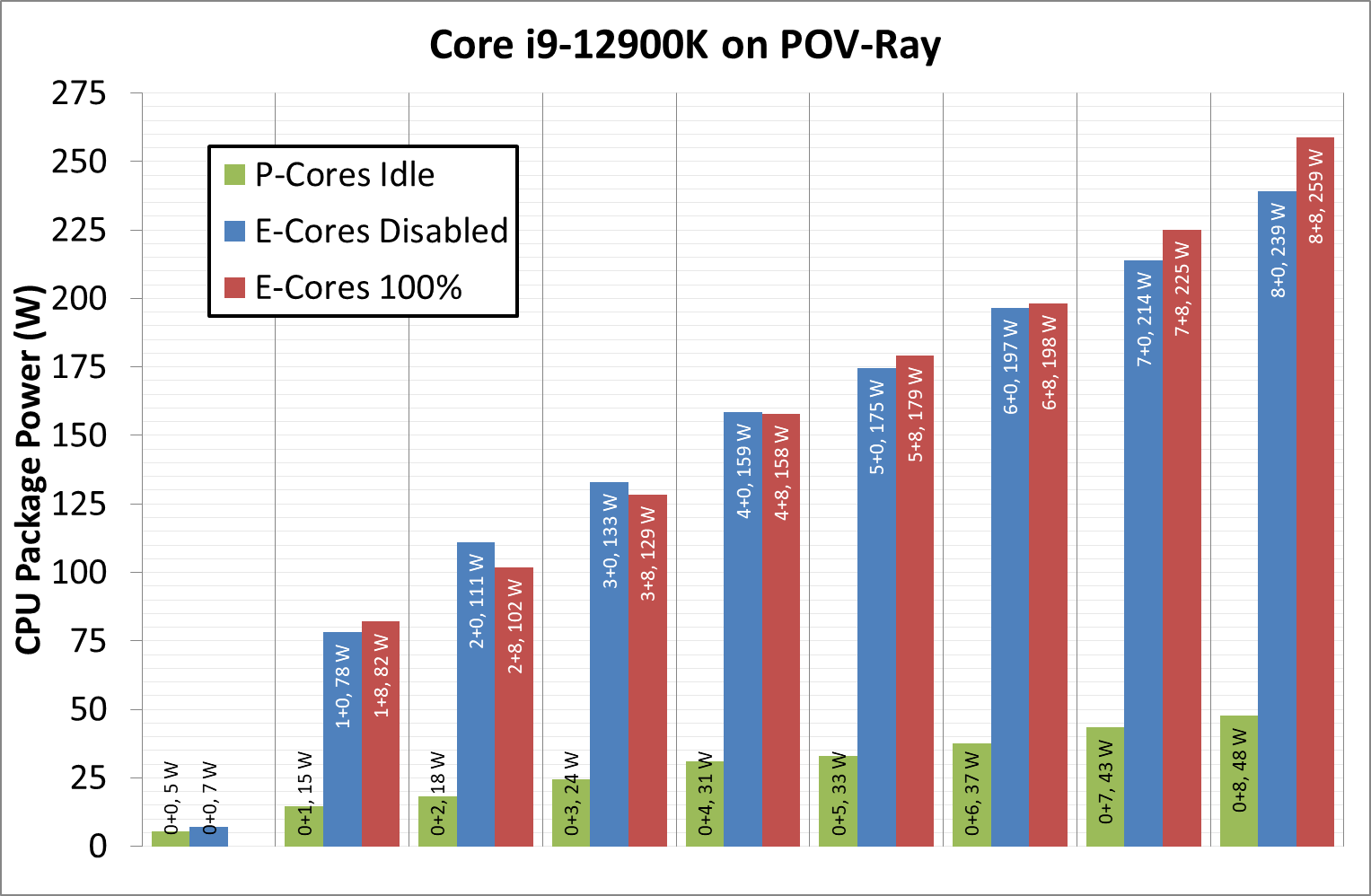
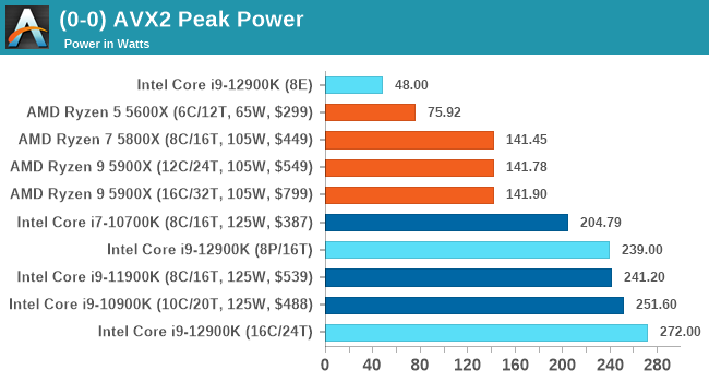
Listed in red, in this test, all 8P+8E cores fully loaded (on DDR5), we get a CPU package power of 259 W. The progression from idle to load is steady, although there is a big jump from idle to single core. When one core is loaded, we go from 7 W to 78 W, which is a big 71 W jump. Because this is package power (the output for core power had some issues), this does include firing up the ring, the L3 cache, and the DRAM controller, but even if that makes 20% of the difference, we’re still looking at ~55-60 W enabled for a single core. By comparison, for our single thread SPEC power testing on Linux, we see a more modest 25-30W per core, which we put down to POV-Ray’s instruction density.
By contrast, in green, the E-cores only jump from 5 W to 15 W when a single core is active, and that is the same number as we see on SPEC power testing. Using all the E-cores, at 3.9 GHz, brings the package power up to 48 W total.
It is worth noting that there are differences between the blue bars (P-cores only) and the red bars (all cores, with E-cores loaded all the time), and that sometimes the blue bar consumes more power than the red bar. Our blue bar tests were done with E-cores disabled in the BIOS, which means that there might be more leeway in balancing a workload across a smaller number of cores, allowing for higher power. However as everything ramps up, the advantage swings the other way it seems. It’s a bit odd to see this behavior.
Moving on to individual testing, and here’s a look at a power trace of POV-Ray in Windows 11:
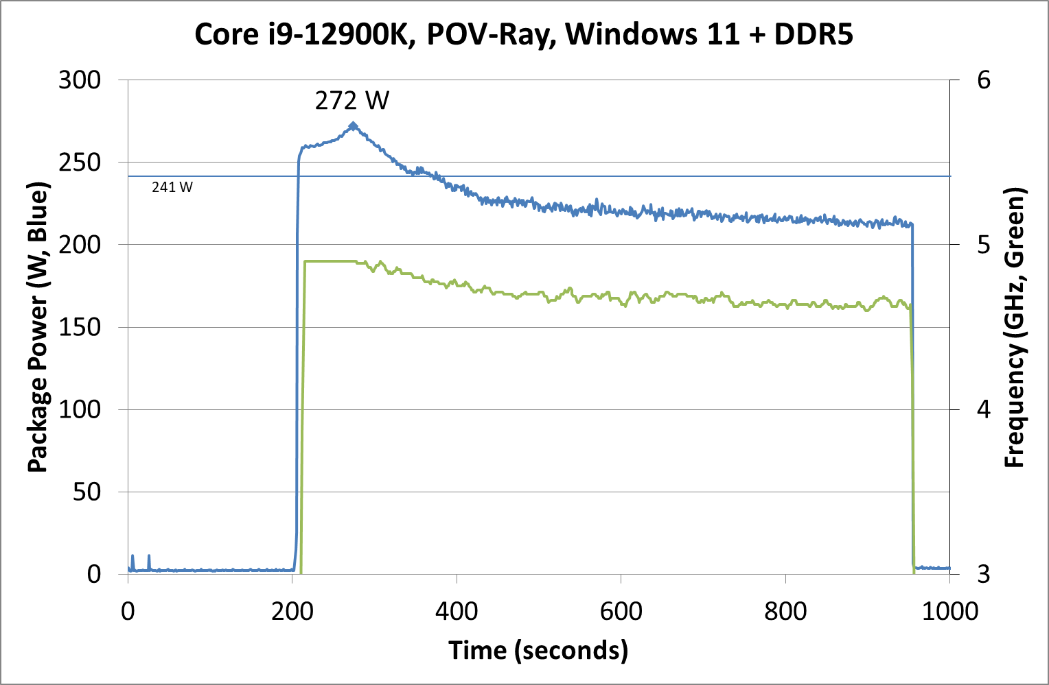
Here we’re seeing a higher spike in power, up to 272 W now, with the system at 4.9 GHz all-core. Interestingly enough, we see a decrease of power through the 241 W Turbo Power limit, and it settles around 225 W, with the reported frequency actually dropping to between 4.7-4.8 GHz instead. Technically this all-core is meant to take into account some of the E-cores, so this might be a case of the workload distributing itself and finding the best performance/power point when it comes to instruction mix, cache mix, and IO requirements. However, it takes a good 3-5 minutes to get there, if that’s the case.
Intrigued by this, I looked at how some of our other tests did between different operating systems. Enter Agisoft:
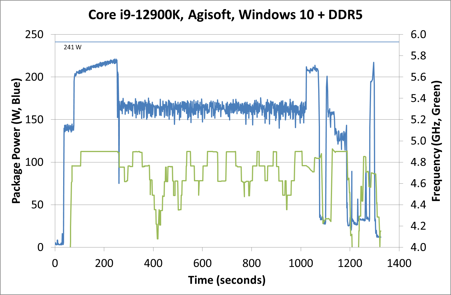
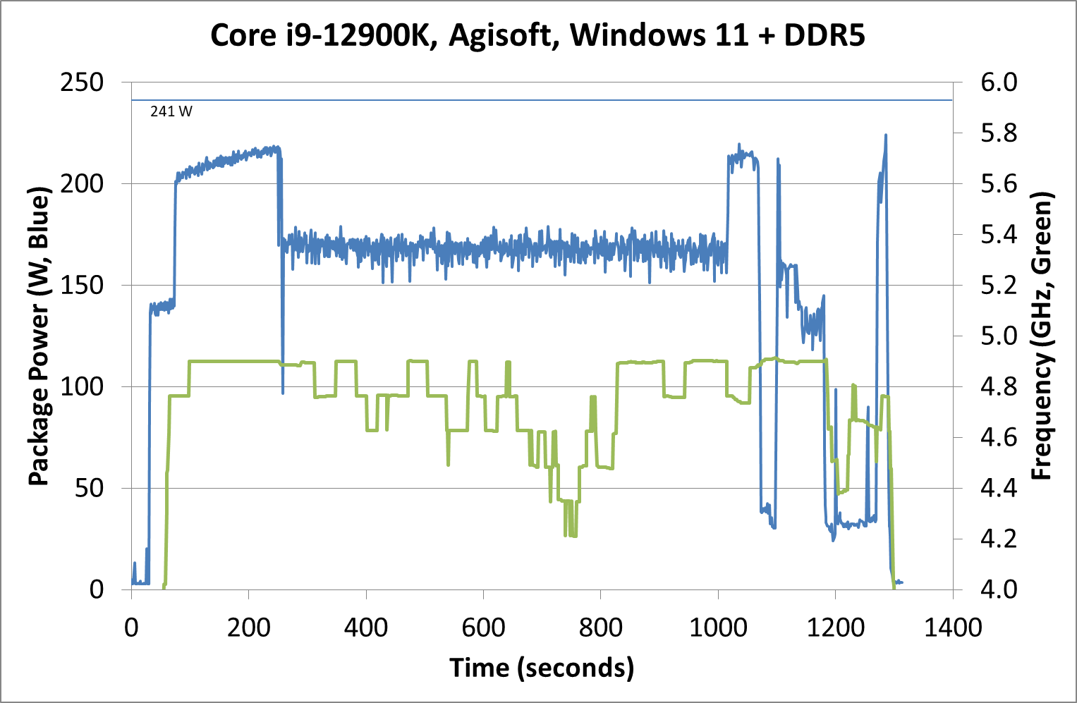
Between Windows 10 and Windows 11, the traces look near identical. The actual run time was 5 seconds faster on Windows 11 out of 20 minutes, so 0.4% faster, which we would consider run-to-run variation. The peaks and spikes look barely higher in Windows 11, and the frequency trace in Windows 11 looks a little more consistent, but overall they’re practically the same.
For our usual power graphs, we get something like this, and we’ll also add in the AVX-512 numbers from that page:
Compared to Intel’s previous 11th Generation Processor, the Alder Lake Core i9 uses more power during AVX2, but is actually lower in AVX-512. The difficulty of presenting this graph in the future is based on those E-cores; they're more efficient, and as you’ll see in the results later. Even on AVX-512, Alder Lake pulls out a performance lead using 50 W fewer than 11th Gen.
When we compare it to AMD however, with that 142 W PPT limit that AMD has, Intel is often trailing at a 20-70 W deficit when we’re looking at full load efficiency. That being said, Intel is likely going to argue that in mixed workloads, such as two software programs running where something is on the E-cores, it wants to be the more efficient design.


474 Comments
View All Comments
mode_13h - Saturday, November 6, 2021 - link
> the only way I think they can remedy this is by designing a new core from scratchI'm not sure I buy this narrative. In the interview with AMD's Mike Clark, he said AMD takes a fresh view of each new generation of Zen and then only reuses what old parts still fit. As Intel is much bigger and better-resourced, I don't see why their approach would fundamentally differ.
> or scaling Gracemont to target Zen 4 or 5.
I don't understand this. The E-cores are efficiency-oriented (and also minimize area, I'd expect). If you tried to optimize them for performance, they'd just end up looking & behaving like the P-cores.
GeoffreyA - Sunday, November 7, 2021 - link
I stand by my view that designing a CPU from scratch will bring benefit, while setting them back temporarily. Of course, am no expert, but it's reasonable to guess that, no matter how much they change things, they're still being restricted by choices made in the Pentium Pro era. In the large, sweeping points of the design, it's similar, and that is exerting an effect. Start from scratch, and when you reach Golden Cove IPC, it'll be at lower power I think. Had AMD gone on with K10, I do not doubt it would never have achieved Zen's perf/watt. Sometimes it's best to demolish the edifice and raise it again, not going to the opposite extreme of a radical departure.As for the E-cores, if I'm not mistaken, they're at greater perf/watt than Skylake, reaching the same IPC more frugally. If that's the case, why not scale it up a bit more, and by the time it reaches GC/Zen 3 IPC, it may well end up doing so with less power. Remember the Pentium M.
What I'm trying to say is, you've got a destination: IPC. These three architectures are taking different routes of power and area to get there. GC has taken a road with heavy toll fees. Zen 3, much cheaper. Gracemont appears to be on an even more economical road. The toll, even on this path, will go up but it'll still be lower than GC's. Zen, in general, is proof of that, surpassing Intel's IPC at a lower point of power.
GeoffreyA - Sunday, November 7, 2021 - link
Anyhow, this is just a generic comment by a layman who's got a passion for these things, and doesn't mean to talk as if he knows better than the engineers who built it.Wrs - Sunday, November 7, 2021 - link
It's not trivial to design a core from scratch without defining an instruction set from scratch, i.e., breaking all backward compatibility. x86 has a tremendous amount of legacy. ARM has quite a bit as well, and growing each year.Can they redo Golden Cove or Gracemont for more efficiency at same perf/more perf at same efficiency? Absolutely, nothing is perfect and there's no defined tradeoff between performance and efficiency that constitutes perfect. But simply enlarging Gracemont to near Golden Cove IPC (a la Pentium M to Conroe) is not it. By doing so you gradually sacrifice the efficiency advantage in Gracemont, and might get something worse than Golden Cove if not optimized well.
The big.LITTLE concept has proven advantages in mobile and definitely has merit with tweaks/support on desktop/server. The misconception you may have is that Golden Cove isn't an inherently inefficient core like Prescott (P4) or Bulldozer. It's just sometimes driven at high turbo/high power, making it look inefficient when that's really more a process capability than a liability.
GeoffreyA - Monday, November 8, 2021 - link
Putting together a new core doesn't necessarily mean a new ISA. It could still be x86.Certainly, Golden Cove isn't of Prescott's or Bulldozer's nature and the deplorable efficiency that results from that; but I think it's pretty clear that it's below Zen 3's perf/watt. Now, Gracemont is seemingly of Zen's calibre but at an earlier point of its history. So, if they were to scale this up slowly, while scrupously maintaining its Atom philosophy, it would reach Zen 3 at similar or less power. (If that statement seems laughable, remember that Skylake > Zen 1, and Gracemont is roughly equal to Skylake.) Zen 3 is right on Golden Cove's tail. So why couldn't Gracemont's descendant reach this class using less power? Its design is sufficiently different from Core to suggest this isn't entirely fantasy.
And the fashionable big/little does have advantages; but question is, do those outweigh the added complexity? I would venture to say, no.
mode_13h - Monday, November 8, 2021 - link
> they're still being restricted by choices made in the Pentium Pro era.No way. There's no possible way they're still beholden to any decisions made that far back. For one thing, their toolchain has probably changed at least a couple times, since then. But there's also no way they're going to carry baggage that's either not pulling its weight or is otherwise a bottleneck for *that* long. Anything that's an impediment is going to get dropped, sooner or later.
> As for the E-cores, if I'm not mistaken, they're at greater perf/watt than Skylake
Gracemont is made on a different node than Skylake. If you backported it to the original 14 nm node that was Skylake's design target, they wouldn't be as fast or efficient.
> why not scale it up a bit more, and by the time it reaches GC/Zen 3 IPC,
> it may well end up doing so with less power.
Okay, so even if you make everything bigger and it can even reach Golden Cove's IPC without requiring major parts being redesigned, it's not going to clock as high. Plus, you're going to lose some efficiency, because things like OoO structures scale nonlinearly in perf/W. And once you pipeline it and do the other things needed for it to reach Golden Cove's clock speeds, it's going to lose yet more efficiency, probably converging on what Golden Cove's perf/W.
There are ways you design for power-efficiency that are fundamentally different from designing for outright performance. You don't get a high-performance core by just scaling up an efficiency-optimized core.
GeoffreyA - Monday, November 8, 2021 - link
Well, you've stumped me on most points. Nonetheless, old choices can survive pretty long. I've got two examples. Can't find any more at present. The instruction fetch bandwidth of 16 bytes, finally doubled in Golden, goes all the way back to Pentium Pro. That could've more related to the limitations of x86 decoding, though. Then, register reads were limited to two or three per clock cycle, going back to Pentium Pro, and only fixed in Sandy Bridge. Those are small ones but it goes to show.I would say, Gracemont is different enough for it to diverge from Golden Cove in terms of perf/watt. One basic difference is that it's using a distributed scheduler design (following in the footsteps of the Athlon, Zen, and I believe the Pentium 4), compared to Pentium Pro-Golden Cove's unified scheduler. Then, it's got 17 execution ports, more than Zen 3's 14 and GC's 12. It's ROB is 256 entries, equal to Zen 3. Instruction boundaries are being marked, etc., etc. It's clock speed is lower? Well, that's all right if its IPC is higher than frequency-obsessed peers. I think descendants of this core could baffle both their elder brothers and the AMD competition.
GeoffreyA - Monday, November 8, 2021 - link
Sorry for all the it's! Curse that SwiftKey!mode_13h - Tuesday, November 9, 2021 - link
> it's got 17 execution portsThat's for simplicity, not by necessity. Most CPUs map multiple different sorts of operations per port, but Gracemont is probably designed in some way that made it cheaper for them just to have dedicated ports for each. I believe its issue bandwidth is 5 ops/cycle.
> It's clock speed is lower? Well, that's all right if its IPC is higher than frequency-obsessed peers.
It would have to be waaay higher, in order to compensate. It's not clear if that's feasible or the most efficient route to deliver that level of performance.
> I think descendants of this core could baffle both their elder brothers and the AMD competition.
In server CPUs? Quite possibly. Performance per Watt and per mm^2 (which directly correlates with perf/$) could be extremely competitive. Just don't expect it to outperform anyone's P-cores.
GeoffreyA - Wednesday, November 10, 2021 - link
I'm out of answers. I suppose we'll have to wait and see how the battle goes. In any case, what is needed is some new paradigm that changes how CPUs operate. Clearly, they're reaching the end of the road. Perhaps the answer will come from new physics. But I wouldn't be surprised there's some fundamental limit to computation. That's a thought.