Intel Discloses Multi-Generation Xeon Scalable Roadmap: New E-Core Only Xeons in 2024
by Dr. Ian Cutress on February 17, 2022 5:30 PM EST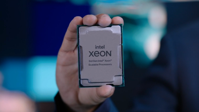
It’s no secret that Intel’s enterprise processor platform has been stretched in recent generations. Compared to the competition, Intel is chasing its multi-die strategy while relying on a manufacturing platform that hasn’t offered the best in the market. That being said, Intel is quoting more shipments of its latest Xeon products in December than AMD shipped in all of 2021, and the company is launching the next generation Sapphire Rapids Xeon Scalable platform later in 2022. Beyond Sapphire Rapids has been somewhat under the hood, with minor leaks here and there, but today Intel is lifting the lid on that roadmap.
State of Play Today
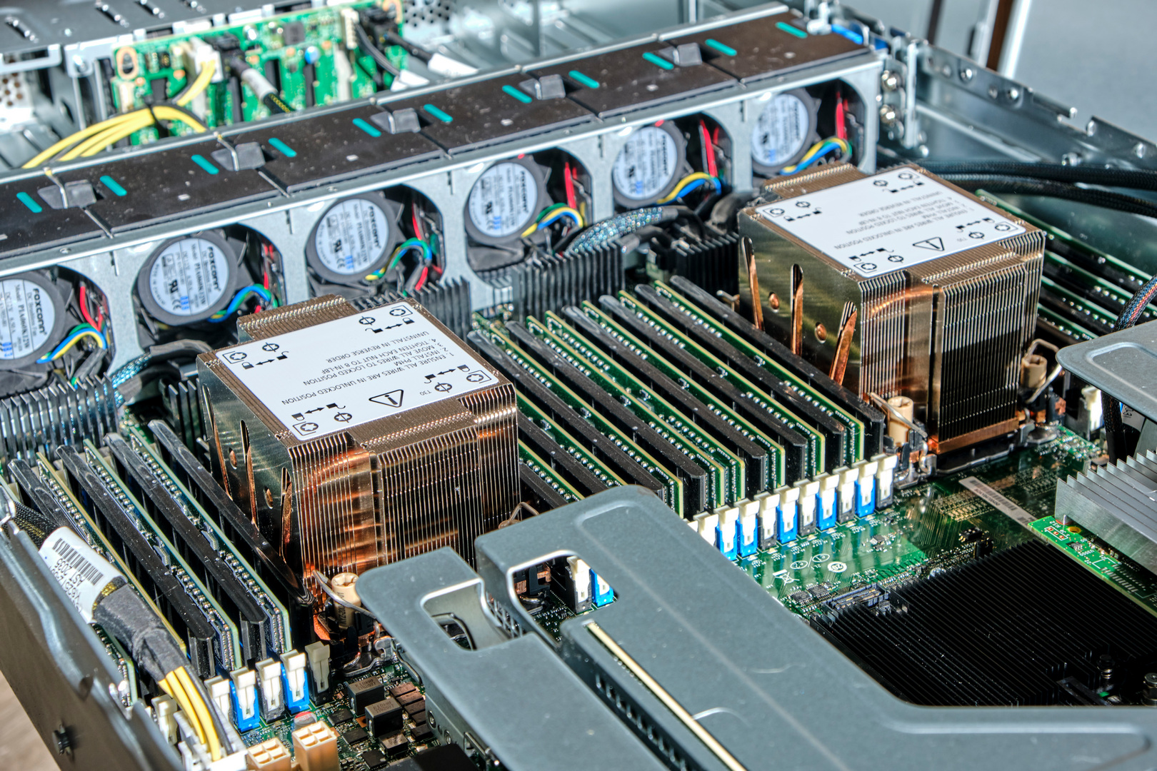
Currently in the market is Intel’s Ice Lake 3rd Generation Xeon Scalable platform, built on Intel’s 10nm process node with up to 40 Sunny Cove cores. The die is large, around 660 mm2, and in our benchmarks we saw a sizeable generational uplift in performance compared to the 2nd Generation Xeon offering. The response to Ice Lake Xeon has been mixed, given the competition in the market, but Intel has forged ahead by leveraging a more complete platform coupled with FPGAs, memory, storage, networking, and its unique accelerator offerings. Datacenter revenues, depending on the quarter you look at, are either up or down based on how customers are digesting their current processor inventories (as stated by CEO Pat Gelsinger).
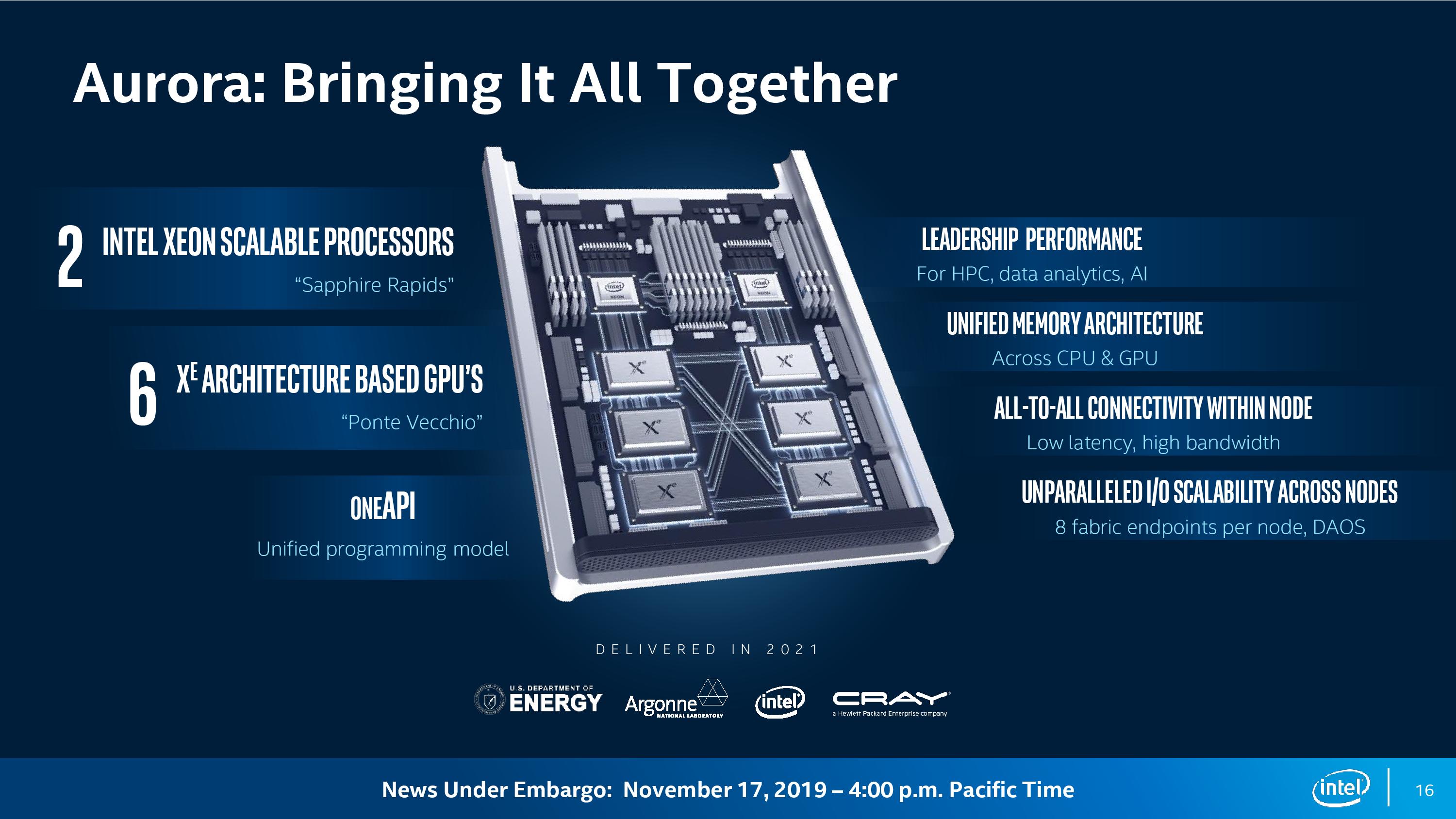
That being said, Intel has put a large amount of effort into discussing its 4th Generation Xeon Scalable platform, Sapphire Rapids. For example, we already know that it will be using >1600 mm2 of silicon for the highest core count solutions, with four tiles connected with Intel’s embedded bridge technology. The chip will have eight 64-bit memory channels of DDR5, support for PCIe 5.0, as well as most of the CXL 1.1 specification. New matrix extensions also come into play, along with data streaming accelerators, quick assist technology, all built on the latest P-core designs currently present in the Alder Lake desktop platform, albeit optimized for datacenter use (which typically means AVX512 support and bigger caches). We already know that versions of Sapphire Rapids will be available with HBM memory, and the first customer for those chips will be the Aurora supercomputer at Argonne National Labs, coupled with the new Ponte Vecchio high-performance compute accelerator.
The launch of Sapphire Rapids is significantly later than originally envisioned several years ago, but we expect to see the hardware widely available during 2022, built on Intel 7 process node technology.
Next Generation Xeon Scalable
Looking beyond Sapphire Rapids, Intel is finally putting materials into the public to showcase what is coming up on the roadmap. After Sapphire Rapids, we will have a platform compatible Emerald Rapids Xeon Scalable product, also built on Intel 7, in 2023. Given the naming conventions, Emerald Rapids is likely to be the 5th Generation.
Emerald Rapids (EMR), as with some other platform updates, is expected to capture the low hanging fruit from the Sapphire Rapids design to improve performance, as well as updates from the manufacturing. With platform compatibility, it means Emerald will have the same support when it comes to PCIe lanes, CPU-to-CPU connectivity, DRAM, CXL, and other IO features. We’re likely to see updated accelerators too. Exactly what the silicon will look like however is still an unknown. As we’re still new in Intel’s tiled product portfolio, there’s a good chance it will be similar to Sapphire Rapids, but it could equally be something new, such as what Intel has planned for the generation after.
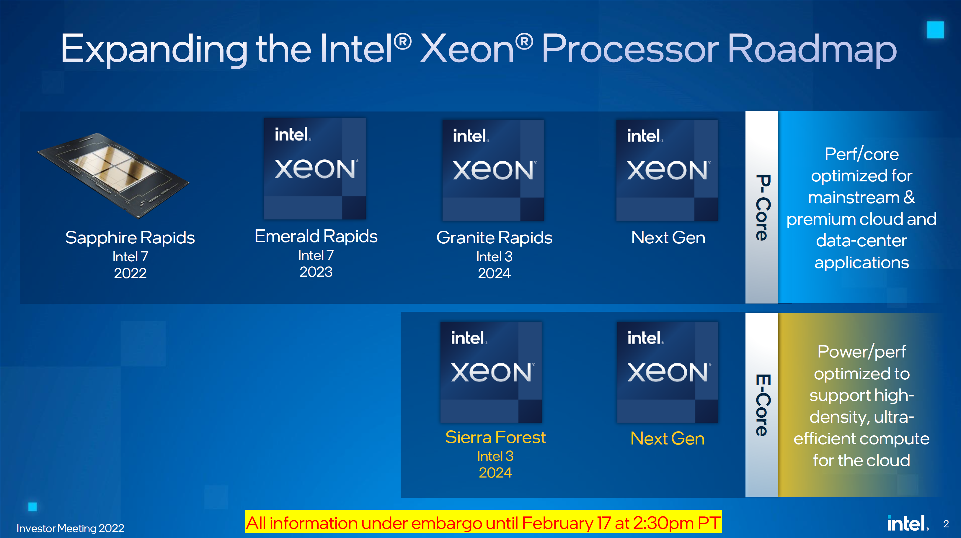
After Emerald Rapids is where Intel’s roadmap takes on a new highway. We’re going to see a diversification in Intel’s strategy on a number of levels.
Starting at the top is Granite Rapids (GNR), built entirely of Intel’s performance cores, on an Intel 3 process node for launch in 2024. Previously Granite Rapids had been on roadmaps as an Intel 4 node product, however, Intel has stated to us that the progression of the technology as well as the timeline of where it will come into play makes it better to put Granite on that Intel 3 node. Intel 3 is meant to be Intel’s second-generation EUV node after Intel 4, and we expect the design rules to be very similar between the two, so it’s not that much of a jump from one to the other we suspect.
Granite Rapids will be a tiled architecture, just as before, but it will also feature a bifurcated strategy in its tiles: it will have separate IO tiles and separate core tiles, rather than a unified design like Sapphire Rapids. Intel hasn’t disclosed how they will be connected, but the idea here is that the IO tile(s) can contain all the memory channels, PCIe lanes, and other functionality while the core tiles can be focused purely on performance. Yes, it sounds like what Intel’s competition is doing today, but ultimately it’s the right thing to do.
Granite Rapids will share a platform with Intel’s new product line, which starts with Sierra Forest (SRF) which is also on Intel 3. This new product line will be built from datacenter optimized E-cores, which we’re familiar with from Intel’s current Alder Lake consumer portfolio. The E-cores in Sierra Forest will be a future generation than the Gracemont E-cores we have today, but the idea here is to provide a product that focuses more on core density rather than outright core performance. This allows them to run at lower voltages and parallelize, assuming the memory bandwidth and interconnect can keep up.
Sierra Forest will be using the same IO die as Granite Rapids. The two will share a platform – we assume in this instance this means they will be socket compatible – so we expect to see the same DDR and PCIe configurations for both. If Intel’s numbering scheme continues, GNR and SRF will be Xeon Scalable 6th Generation products. Intel stated to us in our briefing that the product portfolio currently offered by Ice Lake Xeon products will be covered and extended by a mix of GNR and SRF Xeons based on customer requirements. Both GNR and SRF are expected to have full global availability when launched.
The E-core Sierra Forest focused on core density will end up being compared to AMD’s equivalent, which for Zen4c will be called Bergamo – AMD might have a Zen5 equivalent when SRF comes to market.
I asked Intel whether the move to GNR+SRF on one unified platform means the generation after will be a unique platform, or whether it will retain the two-generation retention that customers like. I was told that it would be ideal to maintain platform compatibility across the generations, although as these are planned out, it depends on timing and where new technologies need to be integrated. The earliest industry estimates (beyond CPU) for PCIe 6.0 are in the 2026 timeframe, and DDR6 is more like 2029, so unless there are more memory channels to add it’s likely we’re going to see parity between 6th and 7th Gen Xeon.
My other question to Intel was about Hybrid CPU designs – if Intel was now going to make P-core tiles and E-core tiles, what’s stopping a combined product with both? Intel stated that their customers prefer uni-core designs in this market as the needs from customer to customer differ. If one customer prefers an 80/20 split on P-cores to E-cores, there’s another customer that prefers a 20/80 split. Having a wide array of products for each different ratio doesn’t make sense, and customers already investigating this are finding out that the software works better with a homogeneous arrangement, instead split at the system level, rather than the socket level. So we’re not likely to see hybrid Xeons any time soon. (Ian: Which is a good thing.)
I did ask about the unified IO die - giving the same P-core only and E-core only Xeons the same number of memory channels and I/O lanes might not be optimal for either scenario. Intel didn’t really have a good answer here, aside from the fact that building them both into the same platform helped customers synergize non-returnable development costs across both CPUs, regardless of the one they used. I didn’t ask at the time, but we could see the door open to more Xeon-D-like scenarios with different IO configurations for smaller deployments, but we’re talking products that are 2-3+ years away at this point.
| Xeon Scalable Generations | ||||||
| Date | AnandTech | Codename | Abbr. | Max Cores |
Node | Socket |
| Q3 2017 | 1st | Skylake | SKL | 28 | 14nm | LGA 3647 |
| Q2 2019 | 2nd | Cascade Lake | CXL | 28 | 14nm | LGA 3647 |
| Q2 2020 | 3rd | Cooper Lake | CPL | 28 | 14nm | LGA 4189 |
| Q2 2021 | Ice Lake | ICL | 40 | 10nm | LGA 4189 | |
| 2022 | 4th | Sapphire Rapids | SPR | * | Intel 7 | LGA 4677 |
| 2023 | 5th | Emerald Rapids | EMR | ? | Intel 7 | ** |
| 2024 | 6th | Granite Rapids | GNR | ? | Intel 3 | ? |
| Sierra Forest | SRF | ? | Intel 3 | |||
| >2024 | 7th | Next-Gen P | ? | ? | ? | ? |
| Next-Gen E | ||||||
| * Estimate is 56 cores ** Estimate is LGA4677 |
||||||
For both Granite Rapids and Sierra Forest, Intel is already working with key ‘definition customers’ for microarchitecture and platform development, testing, and deployment. More details to come, especially as we move through Sapphire and Emerald Rapids during this year and next.


144 Comments
View All Comments
Kamen Rider Blade - Thursday, February 17, 2022 - link
It'll probably be a P-core only feature.E-cores don't have that much die area to work with.
AVX-512 eats up ALOT of die space.
IntelUser2000 - Thursday, February 17, 2022 - link
The server E cores are different from client E cores.Remember Xeon Phi? It took the Silvermont Atom cores and *heavily* modified them. Added AVX-512 too.
Also, AVX-512 on the E cores are going to end up smaller. The Xeon Phi AVX-512 was much smaller than the one on Skylake.
whatthe123 - Thursday, February 17, 2022 - link
if they're looking for MT throughput, shaving some cache/bandwidth might be worth it for AVX-512. It is actually more performant per watt.Calin - Friday, February 18, 2022 - link
But it is dead space if you don't use it, and might be replaced by cache, improved logic units and so on.It could make sense to put AVX-512 only in P-cores Xeons, and leave the "efficiency" market to some other technology (accelerators, GPUs, FPGAs, ...).
Kevin G - Thursday, February 17, 2022 - link
AVX-512 support does need additional and wider registers to function. However, the instructions themselves were designed to be cracked into 256 bit chunks for the execution units to handle. The benefit is that no additional die space has to be used in execution units but the catch is that peak throughput does not change between AVX2 and AVX-512 as the same amount of work is being done per cycle using 256 bit wide SIMD units. There can still be some performance increases due to the additional registers and some efficiency gains with the new instructions but no where near what doubling the execution width would do for SIMD heavy based code.Intel has made a mess of their ISA and it is time for them to clean things up with some standardization.
JayNor - Saturday, February 19, 2022 - link
There were more registers and wider registers added for avx512https://en.wikipedia.org/wiki/AVX-512#Extended_reg...
JayNor - Saturday, February 19, 2022 - link
Intel provides 512 bit fma units for avx512... so they aren't cracking these into 256 bit operations for the FMAs. Their high end server chips have dual avx512 FMA units per core. I've seen reports that the SPR chips, even down to 8 core versions, will all have dual avx512 FMAs per core.https://www.intel.com/content/www/us/en/architectu...
Mike Bruzzone - Sunday, February 20, 2022 - link
mbMike Bruzzone - Sunday, February 20, 2022 - link
mbkpb321 - Thursday, February 17, 2022 - link
I'm kinda surprised the E core only Xeon is so far out. After seeing the performance of 4 E cores in roughly the same die space as one P core for the consumer chips on multithreaded stuff it seemed like such an obvious move. I'd expect the E cores to do even better in servers as they can't run the P cores as high up the power/performance curve in the server chips so they'll loose some of their clock speed advantage.