Intel Goes Full XPU: Falcon Shores to Combine x86 and Xe For Supercomputers
by Ryan Smith on February 17, 2022 2:30 PM EST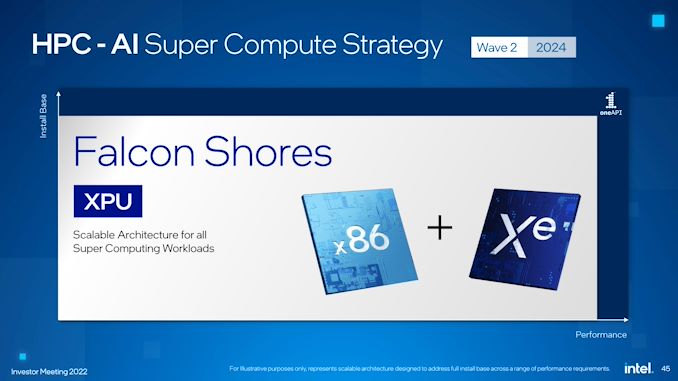
One of Intel’s more interesting initiatives over the past few years has been XPU – the idea of using a variety of compute architectures in order to best meet the execution needs of a single workload. In practice, this has led to Intel developing everything from CPUs and GPUs to more specialty hardware like FPGAs and VPUs. All of this hardware, in turn, is overseen at the software level by Intel’s oneAPI software stack, which is designed to abstract away many of the hardware differences to allow easier multi-architecture development.
Intel has always indicated that their XPU initiative was just a beginning, and as part of today’s annual investor meeting, Intel is finally disclosing the next step in the evolution of the XPU concept with a new project codenamed Falcon Shores. Aimed at the supercomputing/HPC market, Falcon Shores is a new processor architecture that will combine x86 CPU and Xe GPU hardware into a single Xeon socket chip. And when it is released in 2024, Intel is expecting it to offer better than 5x the performance-per-watt and 5x the memory capacity of their current platforms.
At a very high level, Falcon Shores appears to be an HPC-grade APU/SoC/XPU for servers. While Intel is offering only the barest of details at this time, the company is being upfront in that they are combining x86 CPU and Xe GPU hardware into a single chip, with an eye on leveraging the synergy between the two. And, given the mention of advanced packaging technologies, it’s a safe bet that Intel has something more complex than a monolithic die planned, be it separate CPU/GPU tiles, HBM memory (e.g. Sapphire Rapids), or something else entirely.
Diving a bit deeper, while integrating discrete components often pays benefits over the long run, the nature of the announcement strongly indicates that there’s more to Intel’s plan here than just integrating a CPU and GPU into a single chip (something they already do today in consumer parts). Rather, the presentation from Raja Koduri, Intel’s SVP and GM of the Accelerated Computing Systems and Graphics (AXG) Group, makes it clear that Intel is looking to go after the market for HPC users with absolutely massive datasets – the kind that can’t easily fit into the relatively limited memory capacity of a discrete GPU.
A singular chip, in comparison, would be much better prepared to work from large pools of DDR memory without having to (relatively) slowly shuffle data in and out of VRAM, which remains a drawback of discrete GPUs today. In those cases, even with high speed interfaces like NVLink and AMD’s Infinity Fabric, the latency and bandwidth penalties of going between the CPU and GPU remain quite high compared to the speed at which HPC-class processors can actually manipulate data, so making that link as short as physically possible can potentially offer performance and energy savings.

Meanwhile, Intel is also touting Falcon Shores as offering a flexible ratio between x86 and Xe cores. The devil is in the details here, but at a high level it sounds like the company is looking at offering multiple SKUs with different numbers of cores – likely enabled by varying the number of x86 and Xe titles.
From a hardware perspective then, Intel seems to be planning to throw most of their next-generation technologies at Falcon Shores, which is fitting for its supercomputing target market. The chip is slated to be built on an “angstrom era process”, which given the 2024 date is likely Intel’s 20A process. And along with future x86/Xe cores, will also incorporate what Intel is calling “extreme bandwidth shared memory”.
With all of that tech underpinning Falcon Shores, Intel is currently projecting a 5x increase over their current-generation products in several metrics. This includes a 5x increase in performance-per-watt, a 5x increase in compute density for a single (Xeon) socket, a 5x increase in memory capacity, and a 5x increase in memory bandwidth. In short, the company has high expectations for the performance of Falcon Shores, which is fitting given the highly competitive HPC market it’s slated for.
And perhaps most interestingly of all, to get that performance Intel isn’t just tackling things from the raw hardware throughput side of matters. The Falcon Shores announcement also mentions that developers will have access to a "vastly simplified GPU programming model" for the chip, indicating that Intel isn’t just slapping some Xe cores into the chip and calling it a day. Just what this entails remains to be seen, but simplifying GPU programming remains a major goal in the GPU computing industry, especially for heterogeneous processors that combine CPU and GPU processing. Making it easier to program these high throughput chips not only makes them more accessible to developers, but reducing/eliminating synchronization and data preparation requirements can also go a long way towards improving performance.
Like everything else being announced as part of today’s investor meeting, this announcement is more of a teaser for Intel. So expect to hear a lot more about Falcon Shores over the next couple of years as Intel continues their work to bringing it to market.
Source: Intel


28 Comments
View All Comments
brucethemoose - Monday, February 21, 2022 - link
My impression of Optane is that its neither here nor there.It doesn't have the durability or speed or even the cost/GB to replace slow DRAM, and SLC flash is good enough(TM) for the vast majority of non-volatile storage. The niche its useful in is really small.
Photonics, on the other hand, has a much wider range of potential usefulness... depending on how it shakes out.
mode_13h - Monday, February 28, 2022 - link
> a theoretically promising technology that Intel will fsck upI'm a fan of Optane, but how much of its failure can really be attributed to Intel's failure to execute? It simply didn't deliver the promised endurance, meaning it really can't be used like slow DRAM.
The bigger failure was the 3D part. From what I understand, the latest gen Optane is still only 4 layers, which represents the biggest hurdle it has in competing with NAND. That makes it simply too expensive for most storage applications. Is that also due to bad management, or simply a technology that ran out of gas before the competition?
mode_13h - Monday, February 28, 2022 - link
> Then put in a few x86 dies for managementDoes the networking industry want x86 for this? From what I understand, networking gear is one area that MIPS and POWER cores have remained entrenched. If I were using those and looking for something different, I'd go to ARM or RISC-V, rather than x86.
And let's not forget that Altera FPGAs still have ARM cores. So, it's not as if Intel is completely blinded by x86's shortcomings.
> it could be something unique like PCIe over optics that leverages CXL
> to build a flat memory space and handle coherency.
Uh, that seems like a mishmash of buzzwords. But I get the idea of wanting CXL protocol over photonics. If you wanted to do that, I'm sure it'd make more sense to swap out the PHY layer, than try to run PCIe over optical, given how much of PCIe 6.0 signalling seems designed around the limitations and issues of copper.
KurtL - Friday, February 18, 2022 - link
This is an evolution that has been years in the making. First there were the USA pre-exascale systems based on NVIDIA GPUs and IBM POWER8 and POWER9 processors that integrated the CPU in the NVLINK fabric to create a joint memory space. Now you see a similar architecture with Saphire Rapids + Ponte Vecchio in Aurora and AMD Trento + MI250X in Frontier and LUMI. On the other hand Fugaku with its A64fx processors has shown what people in HPC already know for quite a while: there are algorithms that cannot benefit a lot from vector or matrix computations acceleration but can still benefit a lot from GPU-like memory bandwidth. And not only the logically separate memory spaces in current x86-based GPU systems but also the physical separation in systems with unified memory limits the gains that can be obtained in many applications. Now that scalar cores and GPU cores can more easily be combined on a single chip or using the tile/chiplet approach, it is only natural that both are combined in a single socket and linked to joint memory controllers. You can already see the benefits of such an approach in the Apple M1, a chip that in some applications can play way above its league because of the close integration of all compute resources both saving power (as data transport is expensive power wise) and making it more efficient to combine the various compute resources.mode_13h - Monday, February 28, 2022 - link
> You can already see the benefits of such an approach in the Apple M1,> a chip that in some applications can play way above its league because
> of the close integration of all compute resources both saving power
> (as data transport is expensive power wise)
Source? Everyone seems to be holding up the M1 as an example of this or that, but I see these claims backed by little or no data.
I doubt the M1's graphics performance benefits specifically from tight integration between the CPU and GPU, but rather from simply having so much memory bandwidth at the disposal of a powerful iGPU. Lots of focus goes into optimizing APIs and games to work well across separate memory spaces. If it were such a huge liability, we'd see dGPUs hit a wall, before they could reach very high performance levels.
duploxxx - Friday, February 18, 2022 - link
Intel is expecting it to offer better than 5x the performance-per-watt and 5x the memory capacity of their current platforms.that is not so difficult knowing 2 years to come and measuring from its existing Xeon platform which fails to deliver performance... Cascade R and Ice Lake are underperforming and Every one is waiting for the so hyped Sapphire rappids which is already delayed a few times.. lets hope it will still show up 2H2022
Calin - Tuesday, February 22, 2022 - link
Their current platform have "low-memory" and "high-memory" processors (the "L" version I think)The Xeon Platinum 8360h supports 1.12TB, the 8360HL supports 4.5TB.
So, the HL already has 4x memory capacity of the 8360H. Going to 5x is groundbreaking
mode_13h - Monday, February 28, 2022 - link
> that is not so difficult knowing 2 years to comeWe already know roughly what the memory technology landscape will look like, in that time. So, please tell us where they plan to get 5x capacity AND 5x bandwidth (relative to Ice Lake SP).
Rudde - Friday, February 18, 2022 - link
The memory bandwidth can be easily achieved with HBM3, but the memory capacity would require a lot of stacks, I imagine. To that end they could use a hybrid approach with Optane for capacity and HBM3 for bandwidth. The perf/W and core density could be achieved by using E-cores.Calin - Tuesday, February 22, 2022 - link
The "Efficiency" cores have better performance per watt, but not so much better. For a 5x, you need to go to simpler hardware (think 4,000 of GPU-like simple cores instead of 64 large cores).Also, memory access (read, write, synchronization, caches, ...) cost a lot of energy - in some cases comparable to processing itself.