Intel 4 Process Node In Detail: 2x Density Scaling, 20% Improved Performance
by Ryan Smith on June 13, 2022 7:00 AM EST
Taking place this week is the IEEE’s annual VLSI Symposium, one of the industry’s major events for disclosing and discussing new chip manufacturing techniques. One of the most anticipated presentations scheduled this year is from Intel, who is at the show to outline the physical and performance characteristics of their upcoming Intel 4 process, which will be used for products set to be released in 2023. The development of the Intel 4 process represents a critical milestone for Intel, as it’s the first Intel process to incorporate EUV, and it’s the first process to move past their troubled 10nm node – making it Intel’s first chance to get back on track to re-attaining fab supremacy.
Intel’s scheduled to deliver their Intel 4 presentation on Tuesday, in a talk/paper entitled “Intel 4 CMOS Technology Featuring Advanced FinFET Transistors optimized for High Density and High-Performance Computing”. But this morning, ahead of the show, they re publishing the paper and all of its relevant figures, giving us our first look at what kind of geometries Intel is attaining, as well as some more information about the materials being used.
Previously known as Intel’s 7nm process, Intel 4 is Intel’s first time using EUV lithography for their chips. A long time coming, the use of EUV promises both to allow Intel to draw the kind of ever-smaller features needed for more advanced manufacturing nodes, while at the same time letting Intel cut down on the number of manufacturing steps required via today’s multi-patterning DUV techniques. Unusually, Intel finds itself as the final of the big three fabs to tap into EUV – the company passed on EUV for the 10nm generation as they didn’t feel it was ready, and then delays with 10nm and 7nm pushed back Intel’s EUV adoption point significantly. As a result, Intel will get to spring forward on the basis of EUV-driven gains, though they will still have to make up for lost time and TSMC’s experience advantage.
The development of Intel 4 is also a critical juncture for the company, as it finally allows them to move past their troubled 10nm process. While Intel has managed to make something suitable of their 10nm process nodes – especially with their most recent 10nm Enhanced SuperFin variant, which we better know as Intel 7 – it’s not been without entirely too much blood, sweat, and years. Intel believes they tried to do too much all at once with 10nm – both in regards to scaling and in too many new manufacturing techniques – which in turn set them back years as they untangled that mess to find and iterate on what went wrong. Unsurprisingly then, Intel is being a bit less aggressive with their first EUV node, and the company overall has taken a much more modular development approach going forward, allowing for new technologies to be implemented (and, if necessary, debugged) in steps.
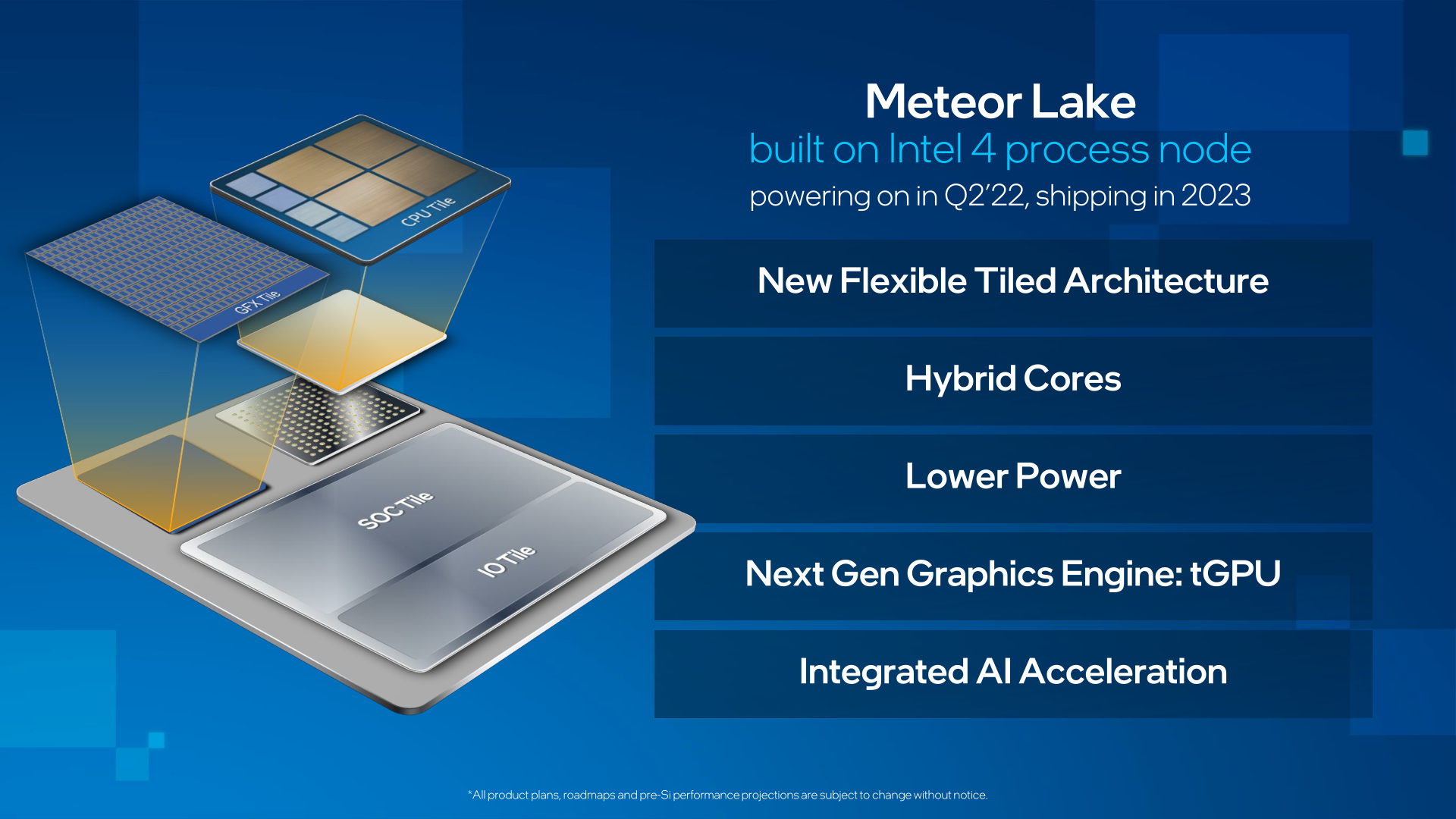
Intel 4, in turn, will be first used for Intel’s forthcoming Meteor Lake client SoC, which is expected to be the basis of Intel’s 14th generation Core processor family. Though not shipping until 2023, Intel already has Meteor Lake up and running in their labs, as per the company’s typical bring-up process. Along with brining a significant bump in process technologies, Meteor Lake will also be Intel’s first tiled/chiplet-based client CPU, using a mix of tiles for I/O, CPU cores, and GPU cores.
Intel 4 Physical Parameters: 2x Density Over Intel 7, Cobalt Use Continues
Diving into the Intel 4 process, Intel has set out to tackle a few different things here. First and foremost is, of course, density. Intel is striving to keep Moore’s Law alive, and while the coinciding death of Dennard scaling means that it’s no longer a simple matter of lighting up twice as many transistors on every generation, a higher transistor density affords smaller chips at with the same hardware, or throwing in more cores (or other processing hardware) with newer desgins.
| Comparing Intel 4 to Intel 7 | |||
| Intel 4 | Intel 7 | Change | |
| Fin Pitch | 30 nm | 34 nm | 0.88 x |
| Contact Gate Poly Pitch | 50 nm | 54/60 nm | 0.83 x |
| Minimum Metal Pitch (M0) | 30 nm | 40 nm | 0.75 x |
| HP Library Height | 240h | 408h | 0.59 x |
| Area (Library Height x CPP) | 12K nm2 | 24.4K nm2 | 0.49 x |
Of the figures Intel is releasing in this week’s paper, the fin pitch on Intel 4 is down to 30nm, 0.88x the size of Intel 7’s 34nm pitch. Similarly, the pitch between contact gates is now 50nm, down from 60nm before. But most significantly, the minimum metal pitch for the lowest layer (M0) is also 30nm, 0.75x the size of the M0 pitch on Intel 7.
Intel’s library height has also been cut down as well. The cell height for the high-performance library on Intel 4 is 240nm, which is only 0.59 x the height of an HP cell on Intel 7.
As a result, Intel is claiming a 2x increase in density for Intel 4 versus Intel 7 – or more specifically, a halving of size for transistors – a traditional, full node’s improvement in transistor density.
Since chips are 2D constructs, the metric Intel uses for this is multiplying the HP cell height by the contacted poly pitch, which is essentially the width of a cell. In that case they get 24,408 nm2 for Intel 7, and a flat 12,000 nm2 for Intel 4, 0.49x the area of the Intel 7-based cell.
Of course, not every type of structure scales by the same factor with a new process node, and Intel 4 is no different. According to the company SRAM cells on Intel 4 are only around 0.77x the size of the same cells on Intel 7. So while standardized logic cells have doubled in density, SRAM density (for equivalent SRAM types) has only improved by 30% or so.
And, unfortunately, while Intel is talking about density with respect to standard cells, they aren’t officially disclosing actual transistor density figures. For now, what Intel is telling us is that the overall transistor density translates well with the 2x figure they’re currently providing. Which, based on what we know about Intel 7 and its 80 million transistors per mm2 density for HP libraries, would place Intel 4's HP libraries at around 160MTr/mm2.
Since these figures are for Intel's lower density high-performance libraries, the obvious follow-up question to that would be what the figures are for high density libraries – which traditionally squeeze things even more in exchange for reduced clockspeeds. However as it turns out, Intel won’t be developing high density libraries for Intel 4. Instead, Intel 4 will be a pure high-performance node, and high-density designs will come with the successive node, Intel 3.
This unusual development comes as a result of Intel’s modularization efforts for process node development. Intel has essentially adopted a tick tock-like strategy for node development over the next half decade or so, with Intel developing an initial node based on a new technology (e.g. EUV or High-NA machines), and then following that up with a more refined/optimized successor. In the case of Intel 4, while it’s doing important pioneering work for EUV within Intel’s fabs, the company’s bigger plans are for Intel 3 to be their long-term, long-lived EUV node.
All of which means that Intel has no need for high-density libraries with Intel 4, since it is slated to be replaced with the more fully-featured Intel 3 within a year or so. And since Intel 3 is design compatible with Intel 4, it’s clear to see how Intel is pushing its own design teams to use the latter process whenever timetables allow. Intel Foundry Services customers will also be a in a similar boat – they can use Intel 4, but IFS is more focused on supplying access to and design help with Intel 3.
Getting back to Intel 4 itself, the new node comes with a significant change to the metal layers as compared to Intel’s 10nm processes. Intel famously replaced copper with cobalt at the lowest layers of its 10nm process, something that the company deemed necessary for transistor longevity (electromigration resistance) reasons. Unfortunately, cobalt isn’t as good from a performance (clockspeed) perspective, and it’s long been suspected that the switch to cobalt was one of the major stumbling blocks in 10nm development for Intel.
For Intel 4, in turn, Intel is taking half a step back. The company is still using cobalt in their processes, but now rather than pure cobalt they are using what they are calling Enhanced Copper (eCu), which is copper cladded with cobalt. The idea behind eCu is to have the best of both words, maintaining the performance of a doped copper metallization layer, while still getting the electromigration resistance benefits of cobalt.
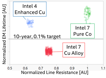
Electromigration lifetimes and line Resistance are compared for different metallurgy options.
And while Intel is no longer using pure cobalt, in some respects their use of cobalt is increasing overall. Whereas Intel’s 10nm processes only used cobalt for the contact gate and first two metal layers, Intel 4 is expanding the use of eCu to the first 5 metal layers. As a result, the lowest-third of the complete metal layer stack in a chip is using Intel’s cobalt-clad copper. Intel has, however, removed cobalt from the gate itself; that’s now pure tungsten, rather than a mix of tungsten and cobalt.
| Intel 4 Metal Stack | ||
| Layer | Metal | Pitch |
| Fin | - | 30 nm |
| Gate | Tungsten | 50 nm |
| Metal 0 | Copper w/Cobalt Cladding | 30 nm |
| Metal 1 | Copper w/Cobalt Cladding | 50 nm |
| Metal 2 | Copper w/Cobalt Cladding | 45 nm |
| Metal 3 | Copper w/Cobalt Cladding | 50 nm |
| Metal 4 | Copper w/Cobalt Cladding | 45 nm |
| Metal 5, 6 | Copper | 60 nm |
| Metal 7, 8 | Copper | 84 nm |
| Metal 9, 10 | Copper | 98 nm |
| Metal 11, 12 | Copper | 130 nm |
| Metal 13, 14 | Copper | 160 nm |
| Metal 15 | Copper | 280 nm |
| Giant Metal 0 | Copper | 1080 nm |
| Giant Metal 1 | Copper | 4000 nm |
All told, the number of metal layers for Intel 4 has increased versus Intel 7. Whereas the latter had 15 metal layers for logic, Intel 4 squeezes in a 16th layer. This is joined by the usual two layers for power routing, which Intel terms its giant layers due to their relatively massive pitches of 1080nm and 4000nm.
Alongside the tighter gate and metal layer pitches, another area where Intel is gaining density improvements from design rule changes for interconnects. With Intel 4, Intel has moved to what they’re calling a gridded interconnect design, which in short, only allows for vias going between metal layers to be placed per a pre-determined grid. Previously, vias could be placed anywhere, which allowed for some flexibility, but had other trade-offs.
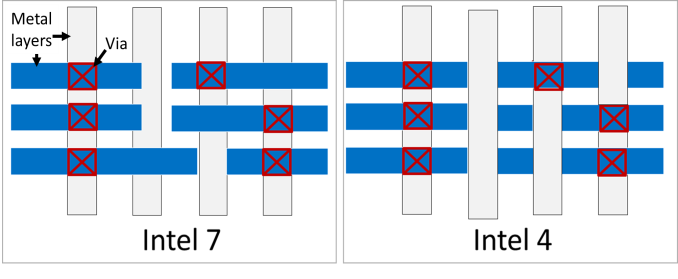
Design rules changed from traditional (left) to gridded (right) to improve yield and improve performance though capacitance reduction
According to Intel, the use of grids has improved both the yields of the process by reducing variability, as well as how they go about optimizing designs. The switch also has a side benefit of allowing Intel to avoid having to use complex, multi-patterned EUV for their interconnects.
Finally, as previously mentioned, the use of EUV is also allowing Intel to reduce the number of steps (and the number of masks) required to fab a chip. While the company isn’t offering absolute numbers, on a relative basis Intel 4 requires 20% fewer masks than Intel 7. Had Intel not done this, the number of masks required would have instead shot up by around 30% due to the number of multi-patterning steps required.
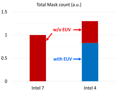
Extensive employment of EUV enables feature scaling and process simplification
The use of EUV is also having a positive impact on Intel’s yields. Though the company isn’t providing exact numbers, the reduction in the number of steps offers fewer opportunities for anything to go wrong that would introduce a defect on a wafer.
Intel 4 Performance: 21.5% More Perf at iso-power/40% Less Power at iso-frequency
Density improvements aside, what kind of performance improvements is Intel seeing for the Intel 4 process? In short, Intel is seeing above-average gains in both frequencies and power efficiency.
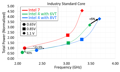
Circuit analysis of industry standard core shows 21.5% performance gain at matched power over Intel 7 at 0.65V. 8VT flow enables 5% performance gain over 6VT at high voltages.
At an iso-power of 0.65v, Intel is seeing a 21.5% increase in clockspeeds attainable versus Intel 7. With that said, 0.65v is at the low end of the curve, and Intel’s graph does show diminishing returns as you go farther up in voltage; at 0.85v and beyond the iso-power gains are closer to 10%. According to Intel, they can squeeze out another 5% or so by using cells designed for higher threshold voltages (8VT), which comes at a cost of higher total power consumption versus standard cells.
And if we take things from the other end, Intel is reporting even larger gains on the power efficiency front with Intel 4. At iso-frequency – in this case around 2.1GHz – Intel is seeing 40% lower power consumption. There are again diminishing returns as frequencies increase (up until Intel 7 hits its practical limits), but it’s more consistent than the performance/frequency gains. This mirrors what we’ve seen with other process nodes – including Intel 7 at its launch – where newer nodes are reducing power consumption at a much greater rate than they’re enabling higher clockspeeds. A full CPU built on the Intel 4 process could conceivably save a great deal of power – so long as you don’t mind it not clocking any higher than before.
All told, the performance gains outlined in Intel’s paper mirror those that they have been claiming up until now, such as the 20% perf-per-watt gains for Intel 4 discussed at last summer’s process roadmap update. For the last year Intel has been approaching the finishing line for Intel 4 development, so as their paper outlines, they appear to be on-track for delivering on their performance gains.
Meanwhile, Intel is also reporting good developments in cost scaling from Intel 7 to Intel 4, though once again the company isn’t providing specific numbers. 1 EUV layer does end up being more expensive than 1 DUV layer, but because EUV eliminates a bunch of multi-patterning, it helps to bring down the total costs by reducing the total number of steps. The switch to EUV is also reducing a bit of the capital pressure on Intel, as Intel 4 doesn’t require quite as much clean room space (though it’s by no means a small amount overall).
Ultimately, as Intel looks to ship Meteor Lake and other first-generation Intel 4 products in 2023, what remains to be seen is how quickly Intel can get their new process node up and running to the standards of high-volume manufacturing. With Meteor Lake samples already in Intel’s labs, Intel is getting ever closer to finally entering the EUV age. But for Intel, hitting all of their goals getting there means not just scaling up production from their Hillsboro development fab, but also mastering the interesting task of replicating their process to Ireland and the other Intel fabs that will be used for Intel 4.


129 Comments
View All Comments
Spunjji - Wednesday, June 15, 2022 - link
It also has abysmal yields!mode_13h - Thursday, June 16, 2022 - link
No disagreement. I just wanted to establish a fact, though its relevance remains unclear (at least to me).Bruzzone - Tuesday, June 14, 2022 - link
drothgery and mode_13th,Thanks for the die size confirmations. My calcs have SF10 at a 20% cost advantage over TSMC 7 and at parity with TSMC 5. Intel achieves this on focused device production in a strategy that necessitates Intel trail one node behind securing and maintaining a downward sloping cost curve on continuing the trailing node depreciation for cost : price / margin advantage as TSMC moves too every next node upward sloping cost curve. On this lagging technique Intel cost is always decreasing as TSMCs cost increases. But if Intel slips two nodes behind the technique looses its parity ability and any leading advantage. I tracked Ice 10, Tiger U and Tiger H SF10 closely in terms of production economics. Some of that production data is here;
https://seekingalpha.com/instablog/5030701-mike-br...
https://seekingalpha.com/instablog/5030701-mike-br...
Tiger U was a quad SF10 validation run there are a ton of them; huge surplus in the channel. My thesis is their characteristics are all over the specification. Tiger H octa was next and then the SR 14C. I don't believe SR is delayed in terms of production readiness but because of business of compute validation irrelevant to the enterprise market on hardware so far ahead of software. Also SR being tough to swallow by the OEM dealer group accustom to Skylake and Cascade lake low price (high volume $400 to $600 on average per unit run end) as Intel kibble good enough to keep business humming along on ow price and availability.
Sapphire Rapids just in the packaging cost is obviously not a low priced product and I think OEMs are having a tough time swallowing SR for the market beyond hyperscale / public cloud business of compute that are not enterprise and mass market of business customers. I also see hyperscale market as monetarily saturated moving to all kinds of acceleration.
For example, how could the big five procure SR in excess of immediate demand knowing they can't resale overage into the secondary market to lower their procurement cost, on hardware so far ahead of software [?] the channel wont buy it ahead of mass market validation.
So does Intel fill the channel following XSL/XCL which is still highly demanded on known stable and low price verse Ice at 10 end generation product? Will Intel respin Ice to SF 10? Will Intel just keep producing Cascade Lake for the masses. Will OEMs take SR knowing software whole product voids and a risky price.
See my comment line for Xeon today channel sales trend observations:
https://seekingalpha.com/user/5030701/comments
Mike Bruzzone, Camp Marketing
mode_13h - Tuesday, June 14, 2022 - link
> rebranded 7nm can actually mass-produce a die larger than Tiger Lake Quad?Tiger Lake was/is produced on Intel 10 nm SuperFin (rebranded as "Intel 10", formerly called 10 nm++). Tiger Lake H exists and is a 8-core part, as @drothgery said.
> The delays on Sapphire Rapids tells us the yield for large dies still sucks for Superfin.
SPR, like ADL, is made on Intel 10 nm Enhanced Super Fin (rebranded as "Intel 7", formerly Intel 10 nm+++).
Bruzzone - Wednesday, June 15, 2022 - link
Mode_13th, writing off SR so said delayed on yield [?] is a traditional thesis, low yield high cost.But consider 4 die at a very manufacturable 350 mm^2. They're not XCC. I acknowledge yield remains a question. I personally believe the package is damn expensive and the component validated in a non production environment, initially, focused on business of compute workloads recommendation systems and OLTP that's general enough and overlap with private / public cloud virtualized storage and server but that's not the general enterprise business market. SR has been in risk production since q3 2021 on my take supporting DDR5 validation and so has Genoa since q3 2021 memory had to have more than a simulator.
Subsequently my SR thesis is 1) the product is not whole as of yet outside business of compute applications, and 2) Intel OEM dealer group can't sell a less than whole platform; hardware ahead of software and, 3) the price low yield or otherwise is excessive for what Skylake and Cascade Lake provide for systems integration channel on corporate enterprise standardized compute.
So what fills the channel if not for XSL, XCL continuing? My answer is large cache Milan verse cache starved Skylake and Cascade Lake+r albeit AMD would have to aggressively supply Milan which I think is about to ramp the XSL XCL replacement market is to big to ignore. McNamara said Milan production would continue at AMD financial analyst day. I considered that the most important statement of AMD's public disclosure.
Finally, I give Intel [more] credit for getting its fabrication act together observing TL U to H. Alder is on same process as SR and Alder so said by Intel surpassing 15 M units of production. Intel for decades loves to produce around 245mm^2 consumer market components and 14/12nm HCC around 400 mm^2 was highly manufacturable granted a different process.
Intel can do stupid things, make decisions that lack integrity and definitively has made severe errors but I never count them out. Ice volume in the channel increased 16% in last nine weeks and splits channel market share on available volume with Milan. Ice is not SF10/7 but the predecessor fin fet process compound weekly channel supply volume growth is 6% per week over 59 weeks begins March 31. Intel says 4 M Ice have sold which is not a large volume for mainstay Xeon and I believe its because 1) market is standardized on XSL/XCL, 2) Ice is not SF10 and run end, 3) Its not whole for the mass market on hardware ahead of software.
This is what the market is currently buying XSL + XCL by core grade SKU sales trend last nine weeks;
4C = 1.86% supply + 24.2% gain last nine week (trade in)
6C = 1.86% + 9.7%
8C = 12.26% < 38.2% shows a sweet spot
10C = 7.89% < 45% shows applications by core sweet spot
12C = 11.04% < 20.7%
14C = 11,89% < 40.09% sweet spot
16C = 11.78% < 8.5%
18C = 6.8% + 20.6% trade in
20C = 9.51% < 14.9% applications sweet spot enters virtual
22C = 2.26% + 1.4%
24C = 8.31% < 2.1%
26C = 2.08% + 2%
28C = 12.44% + 4.4% (virtual environment)
Xeon Ice full line at 10 over 1st 59 weeks CWG (channel supply volume) = 6%
Xeon Cascade Lake at 14/12 over 1st 59 weeks = 71.9% that's telling
Xeon Ivy Bridge, 22 nm out the gate was difficult over 1st 59 weeks = 4.6%
Xeon Haswell, 22 nm was easy out the gate over 1st 59 weeks = 33.87%
Result; Ice looks like a v2 out the gate.
Broadwell quad Crystal Well 14 nm tough out the gate 1st 59 weeks = 1%
Ice U quad at 10 over 59 weeks CWG (channel supply volume) = 19.8%
Tiger U quad SF10/7 over 59 weeks CWG = 15.9%
Tiger H octa SF10/7 over 50 weeks run to date CWG = 13.6%
Alder S i9/i7/i5 only over 30 weeks rune to date CWG = 64.8% Intel's producing on SF10/7
We can look at another Ice supply aspect;
P40C = 4.91% full run to date supply and + 53% in the prior 9 weeks
P38C = 2.09% + 300%
P36C = 5.98% + 170%
P32C = 10.18% + 70%
G32C = 7.53% + 192%
G28C = 14.60% + 74%
G26C = 2.15% < 60%
G24C = 7.29% + 89%
G20C = 0.26% and n/a currently
G18C = 4.31% + 12.5%
G16C = 6.53% + 26%
G12C = 1.75% < 60%
G8C = 3.57% + 166%
All Silver = 25.51% + 37%
All W = 3.34% < 40%
Milan volume in the channel grew 33% in the prior nine weeks and on a compound weekly basis at 10.8% over 49 consecutive weeks beginning June 19, 2021. I have Milan production at 9,644,933 units to date which is a lot for AMD.
We can look at another Milan supply aspect;
64C = 35.21% full run to date supply and + 19.5% in the prior 9 weeks
56C = 3.67% + 11%
48C = 3.62% + 420%
32C = 18.21% + 91%
28C = 2.66% + 34%
24C = 20.26% + 19.6%
16C = 14.05% + 58.8%
8C = 2.33 < 16.7%
G20C = 0.26% and n/a currently
G18C = 4.31% + 12.5%
G16C = 6.53% + 26%
G12C = 1.75% < 60%
G8C = 3.57% + 166%
All Silver = 25.51% + 37%
All W = 3.34% < 40%
Okay, Xeon Ice is being supplied similar to Ivy v2 that had a slow start. But Alder is yielding and 90% of volume are i9/i7 all else is organic fall out from sort. My thesis remains. Sapphire Rapids package is costly. SR hardware is ahead of general market applications software. Intel OEMs are bocking at procurement price and the ability to sell other than to 'business of compute' in question minimally on SR not yet validated in the general use market. No hyperscale public cloud operation will want Intel dealer group as its master distributor a direct Intel CPU sales environment primarily.
SR currently comes with costs that are not fully understood.
Mike Bruzzone, Camp Marketing
Speedfriend - Monday, June 13, 2022 - link
surely 20% perf per watt gains isnt going to get them anywhere near where Apple is now. Will they get more out of the design side?Jorgp2 - Monday, June 13, 2022 - link
Do you not understand that this is for the manufacturing node, not the actual end product?mode_13h - Tuesday, June 14, 2022 - link
Well yes. But, in order to beat that, Intel would mostly have to build a lower-clocking chip, which isn't likely. They might be able to find a few other little power savings here and there, but the main power savings usually comes from the process node.mode_13h - Wednesday, June 15, 2022 - link
Then again, it's probably safe to assume they're not going to build the same chip they have today that merely clocks 20% higher. So, we should expect them to invest some of the efficiency gains in wider structures, better scheduling, or more cache. And that could conceivably deliver more than 20% performance, at ISO-power. However, at ISO-clocks, such a chip would lose much of the 40% power savings.HelloThere33 - Monday, June 13, 2022 - link
No, but the 40% less power for same perf will