Intel's Xeon E5-2600 V2: 12-core Ivy Bridge EP for Servers
by Johan De Gelas on September 17, 2013 12:00 AM EST
The core architecture inside the latest Xeon is typically a step behind what you find inside the latest desktop and notebook chips. A longer and more thorough validation is one reason, but there is more. The high-end model of the Xeon E5-2600 V2 or "Ivy Bridge EP" is, aside from the core architecture, completely different from the Ivy-bridge "i7 \-3xxx" that was launched in the spring of last year. With up to twelve cores, two integrated memory controllers, no GPU and 30MB L3 cache, it is the big brother of the recently reviewed Ivy-bridge E (Core i7-4960X). Intel has three die flavors of the Ivy-bridge EP:
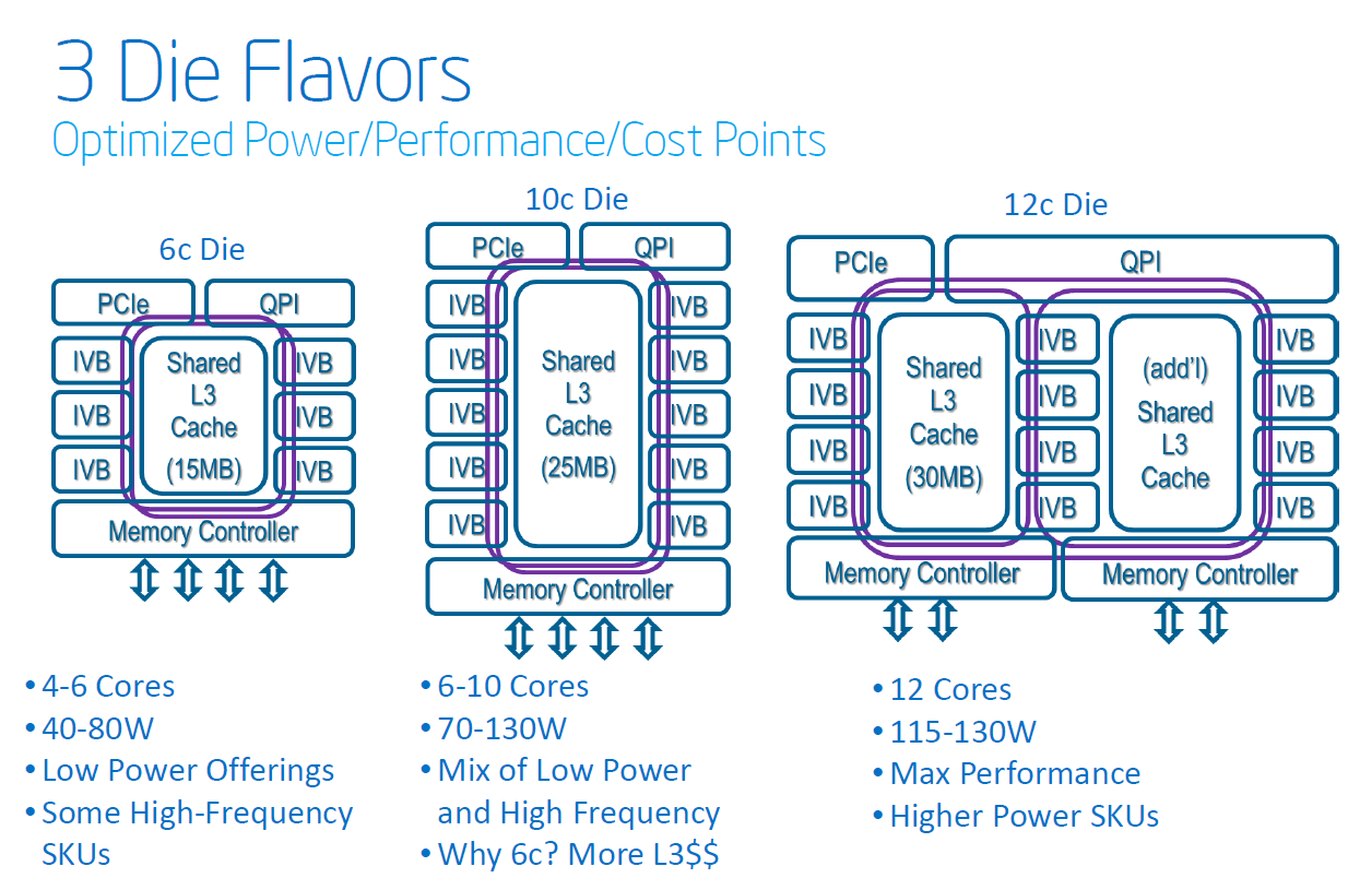
The first one is the one with the lowest core count (4/6 cores), which is found in SKUs targeted at the workstation and enthusiast market (high frequencies) or low power SKUs; this is the core being used in the enthusiast Ivy Bridge-E processors. The second one is targeted at the typical server environment with higher core counts (6 to 10 cores) and a larger L3 cache (25MB). The third and last one is the high performance HPC and server die, with 12 cores, two memory controllers for lower memory latency, and 30MB of L3 cache.
The cool thing about the newest Xeon E5 processors is that they run on the same Romley EP platform as LGA-2011 chips. This should save the OEMs a lot of time and money, and hopefully these savings will trickled down to the customers. Let's see how Intel's latest server update performs, and if it manages to impress more than the enthusiast Ivy Bridge-E.


70 Comments
View All Comments
Kevin G - Tuesday, September 17, 2013 - link
I'd be careful about using Java benchmarks on those SPARC chips for an overall comparison. The results on the SPARC side are often broken.x86 for many years has been ahead of SPARC. Only with the most recent chips has Oracle produced a very performance competitive chip.
The only other architecture that out runs Intel's best x86 chips is the POWER7/POWER7+. When the POWER8 ships, it is expected to be faster still.
Brutalizer - Thursday, September 19, 2013 - link
@Kevin G"...The results on the SPARC side are often broken..."
What do you mean with that? The Oracle benchmarks are official and anyone can see how they did it. Regarding the SPARC T5 performance, it is very fast, typically more than twice as fast as Xeon cpus. Just look at the official, accepted benchmarks on the site I linked to.
Kevin G - Friday, September 20, 2013 - link
@BrutalizerThere is a SPEC subtest whose result on SPARC is radically higher than other platforms. The weight of this one test affects the overall score. It has been a few years since I read up about this and SPARC as a platform has genuinely become performance competitive again.
Phil_Oracle - Friday, February 21, 2014 - link
Are you talking about libquantum?http://www.spec.org/cpu2006/Docs/462.libquantum.ht...
I believe IBM is the worst culprit on this subtest, showing a significant difference between base and peak. More so than any other vendor.
http://www.spec.org/cpu2006/results/res2012q4/cpu2...
But today, I believe all vendors have figured out how to improvise (cheat) on this test, even Xeon based.
http://www.spec.org/cpu2006/results/res2014q1/cpu2...
That’s why I believe SPEC CPU2006 is outdated and needs replacing and suggest looking at more realistic, recent (dal world) benchmarks like SPECjbb2013, SPECjEnterprise2010 or even TPC-H.
Phil_Oracle - Friday, February 21, 2014 - link
x86 was clearly ahead of SPARC till about SPARC T4 timeframe when Oracle took over R&D on SPARC. SPARC T4 allowed Oracle to equalize the playing field, especially in areas like database where the SPARC T4 really shines and shows considering many of the world record benchmarks that where released. When SPARC T5 came out last year, it increased performance by 2.4x, clobbering practically every other CPU out there. Today, you'll be hard pressed to find a real world benchmark, ones that are fully audited, where SPARC T5 is not in a leadership position, whether java based like SPECjbb2013 or SPECjEnterprise2010 or database like TPC-C or TPC-H.psyq321 - Tuesday, September 17, 2013 - link
I know that EX will be using the (scalable) memory buffer, which is probably the main reason for the separate pin-out. I guess they could still keep both memory controllers in, and fuse the appropriate one depending if it is an EX or EP SKU, if this would still make sense from a production perspective.Kevin G - Tuesday, September 17, 2013 - link
It wouldn't make much sense as the EX line up moves the DDR3 physical interface off to the buffer chip. There is a good chunk of die space used for the 256 bit wide memory interface in the EP line. Going the serial route, the EX line is essentially doubling the memory bandwidth while using the same number of IO pins (though at the cost of latency).The number of PCIe lanes and QPI links also changes between the EP and EX line up. The EP has 40 PCIe lanes where as the EX has 32. There are 4 QPI links on the EX line up making them ideal for 4 and 8 socket systems were as the EP line has 2 QPI links good for dual or a poor quad socket configuration.
psyq321 - Wednesday, September 18, 2013 - link
Hmm, this source: http://www.3dcenter.org/news/intel-stellt-ivy-brid...Claims that HCC is 12-15 core design. They also have a die-shot of a 15 core variant.
Kevin G - Thursday, September 19, 2013 - link
I'll 1-up you: Intel technical reference manuals (PDF).http://www.intel.de/content/dam/www/public/us/en/d...
http://www.intel.de/content/dam/www/public/us/en/d...
It does appear to be 15 core judging from the mask in the CSR_DESIRED_CORES register.
However, there is not indication that the die supports serial memory links to a buffer chip or >3 QPI links that an EX chip would have.
psyq321 - Thursday, September 19, 2013 - link
Well, I guess without Intel openly saying or somebody laser-cutting the die it would not be possible to know exactly is it a shared die between HCC EP and EX.However, there are lots of "hints" that the B-package Ivy Bridge EP hide more cores, like the ones you linked. If it is the case, it is really a shame that Intel did not enable all cores in the EP line. There would still be lots of places for differentiation between the EX and EP lines, since EX anyway contains RAS features without which the target enterprise customers would probably not even consider EP, even if it had the same number of cores.
Also, Ivy EX will have some really high TDP parts.