AMD Kaveri Review: A8-7600 and A10-7850K Tested
by Ian Cutress & Rahul Garg on January 14, 2014 8:00 AM ESTLlano, Trinity and Kaveri Die: Compared
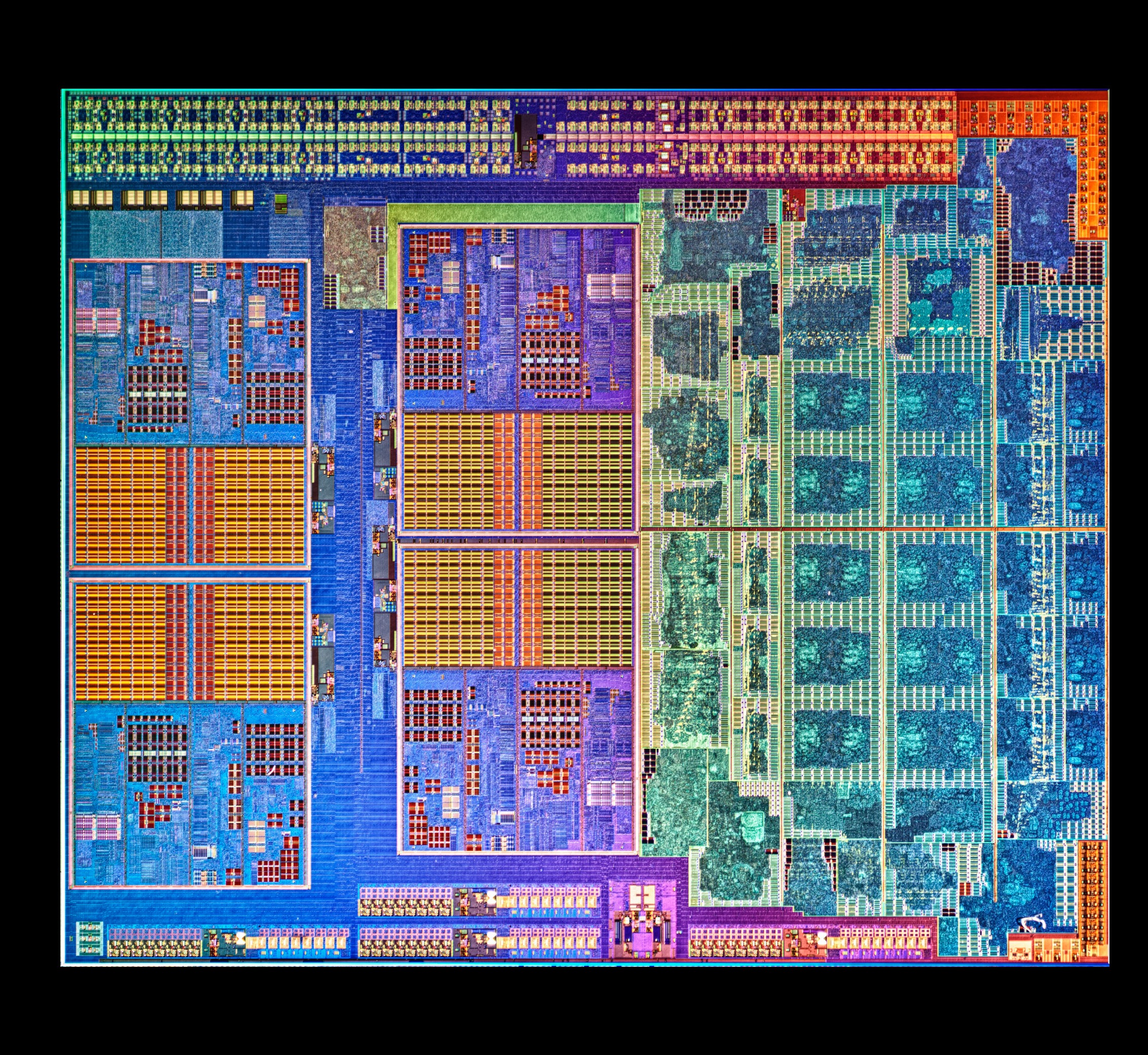
AMD sent along a high res shot of Kaveri's die. Armed with the same from the previous two generations, we can get a decent idea of the progression of AMD's APUs:
Llano, K10 Quad Core

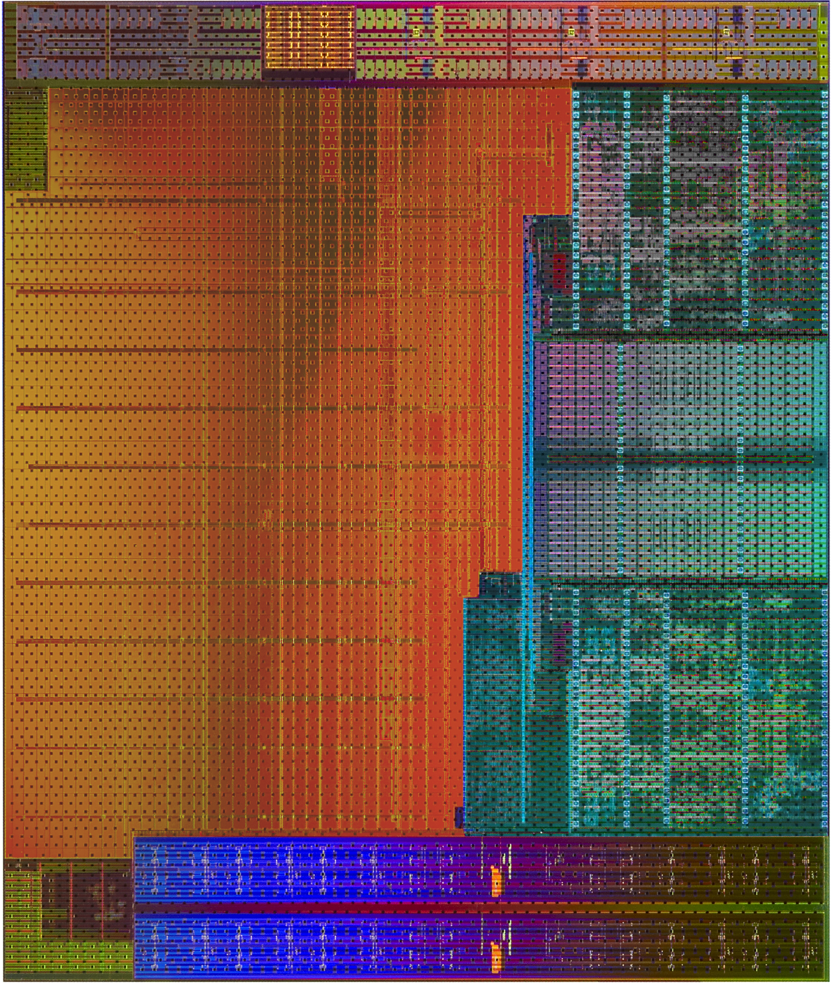
Trinity and Richland Die, with two Piledriver modules and processor graphics
Kaveri, two modules and processor graphics
Moving from Llano to Trinity, we have the reduction from a fully-fledged quad core system to the dual module layout AMD is keeping with its APU range. Moving from Richland to Kaveri is actually a bigger step than one might imagine:
| AMD APU Details | ||||
| Core Name | Llano | Trinity | Richland | Kaveri |
| Microarch | K10 | Piledriver | Piledriver | Steamroller |
| CPU Example | A8-3850 | A10-5800K | A10-6800K | A10-7850K |
| Threads | 4 | 4 | 4 | 4 |
| Cores | 4 | 2 | 2 | 2 |
| GPU | HD 6550 | HD 7660D | HD 8670D | R7 |
| GPU Arch | VLIW5 | VLIW4 | VLIW4 | GCN 1.1 |
| GPU Cores | 400 | 384 | 384 | 512 |
| Die size / mm2 | 228 | 246 | 246 | 245 |
| Transistors | 1.178 B | 1.303 B | 1.303 B | 2.41 B |
| Power | 100W | 100W | 100W | 95W |
| CPU MHz | 2900 | 3800 | 4100 | 3700 |
| CPU Turbo | N/A | 4200 | 4400 | 4000 |
| L1 Cache |
256KB C$ 256KB D$ |
128KB C$ 64KB D$ |
128KB C$ 64KB D$ |
192KB C$ 64KB D$ |
| L2 Cache | 4 x 1MB | 2 x 2 MB | 2 x 2 MB | 2 x 2 MB |
| Node | 32nm SOI | 32nm SOI | 32nm SOI | 28nm SHP |
| Memory | DDR-1866 | DDR-1866 | DDR-2133 | DDR-2133 |
Looking back at Llano and Trinity/Richland, it's very clear that AMD's APUs on GF's 32nm SOI process had a real issue with transistor density. The table below attempts to put everything in perspective but keep in mind that, outside of Intel, no one does a good job of documenting how they are counting (estimating) transistors. My only hope is AMD's transistor counting methods are consistent across CPU and GPU, although that alone may be wishful thinking:
| Transistor Density Comparison | ||||||||
| Manufacturing Process | Transistor Count | Die Size | Transistors per mm2 | |||||
| AMD Kaveri | GF 28nm SHP | 2.41B | 245 mm2 | 9.837M | ||||
| AMD Richland | GF 32nm SOI | 1.30B | 246 mm2 | 5.285M | ||||
| AMD Llano | GF 32nm SOI | 1.178B | 228 mm2 | 5.166M | ||||
| AMD Bonaire (R7 260X) | TSMC 28nm | 2.08B | 160 mm2 | 13.000M | ||||
| AMD Pitcairn (R7 270/270X) | TSMC 28nm | 2.80B | 212 mm2 | 13.209M | ||||
| AMD Vishera (FX-8350) | GF 32nm SOI | 1.2B | 315 mm2 | 3.810M | ||||
| Intel Haswell 4C (GT2) | Intel 22nm | 1.40B | 177 mm2 | 7.910M | ||||
| NVIDIA GK106 (GTX 660) | TSMC 28nm | 2.54B | 214 mm2 | 11.869M | ||||
If AMD is indeed counting the same way across APUs/GPUs, the move to Kaveri doesn't look all that extreme but rather a good point in between previous APUs and other AMD GCN GPUs. Compared to standalone CPU architectures from AMD, it's clear that the APUs are far more dense thanks to big portions of their die being occupied by a GPU.


380 Comments
View All Comments
PolarisOrbit - Tuesday, January 14, 2014 - link
In the GPU benchmarks the charts were all divided into categories "Performance," "Quality," and "Xtreme." I went back to Testing Platform page to discern what these meant but it didn't say. Any clues?Ryan Smith - Tuesday, January 14, 2014 - link
Check the first page of the GPU performance section; it goes over the different categories.Th-z - Tuesday, January 14, 2014 - link
Nice review and very nice info from Rahul. Questions and comments:1. Not sure why you guys think this should be called SoC. Its MB still has a southbridge and other components to make a complete system.
2. Page 2, first paragraph: "Apple’s Mac Pro dream" and "by doing the dream on a single processor". What is the "dream" you are referring to?
3. Page 9, Table "Intel TestBed", i7s should be 4C/8T.
4. Don't you guys think it's odd that how close 95 W A10-7850K compares to 65 W A8-7600 and 45 W A8-7600 in gaming? With 33.3% more SP, it should have more noticeable increase in FPS. We see better spread with Richland, yet all three of Kaveri are so close to each other, which really makes 7850K unattractive with more than double the TDP compares to 7600 at 45 W.
Could it be it may have been bottlenecked by memroy bandwidth? Sooner or later AMD would need to do their own embedded RAM or putting GDDR5 on MB -- the world's first user configurable GDDR5 on MB, that would be something.
T1beriu - Tuesday, January 14, 2014 - link
4. Could it be because all of them have the same 512 core GPU clocked at the same speed of 720Mhz?T1beriu - Tuesday, January 14, 2014 - link
Nope, I'm just blind.ws3 - Tuesday, January 14, 2014 - link
The Iris Pro results have got to be very worrying for AMD.Yes, Intel is still behind in integrated graphics, but they are improving by leaps and bounds, and their CPU performance is miles ahead of AMD.
I loved my Athlons, but I think AMD is on the verge of having nothing to offer.
UtilityMax - Tuesday, January 14, 2014 - link
Iris Pro is basically a proof that Intel can respond to AMD if the APU market does take off. Right now Iris Pro graphics are too expensive, but they could eventually move it onto the same die shared with a lower end i3 CPU.thomascheng - Wednesday, January 15, 2014 - link
AMD already proven they can make a bigger core. Just look at the PS4 and Xbox One. I think while Intel can have the performance crown, only a small percentage will actually buy it.andrewaggb - Wednesday, January 15, 2014 - link
The shame is that AMD should have released an APU similiar to the Pro. They have the tech, the drivers, mantle coming, the gaming deals... to actually pull it off. The biggest problem with iris pro (besides price) is that intel drivers suck. AMD drivers (at least in single gpu scenerios) work well. I think releasing cheap apu's is a good move as well, but at least one high end model would have been good. I think it would sell reasonably well if it could get 60fps at 1080p (ps4 level perf). I don't even think it has to be all that cheap, should be worth at least $100 premium. It enables new possibilities and smaller/quiter form factors. People like that.khanov - Tuesday, January 14, 2014 - link
As you hinted at several times in your article, I think we could see even better iGPU performance from Kaveri with increasing memory bandwidth. I wonder if you might be interested in benchmarking some games at different memory frequency settings up to (and beyond?) DDR3-2400?I personally was hoping that Kaveri might launch with a quad-channel DDR3 memory controller. Yes it would require a new socket and the added signal routing complexity would push up board prices a bit. However, as FM2+ boards are so cheap, I don't see that as a big issue really.
You also asked if anyone would be interested in a XBox One/PS4 style APU with significantly more GPU cores. Well I would! But again, that memory bandwidth issue needs to be resolved.
Something like a six layer mini ITX board with 8GB of GDDR5 soldered underneath (where else would there be room to put it?) would be the brilliant if coupled with a PS4 style APU. It's a nice dream.
Thanks for the very in-depth review. It was a pleasure to read.