AMD Kaveri Review: A8-7600 and A10-7850K Tested
by Ian Cutress & Rahul Garg on January 14, 2014 8:00 AM ESTLlano, Trinity and Kaveri Die: Compared
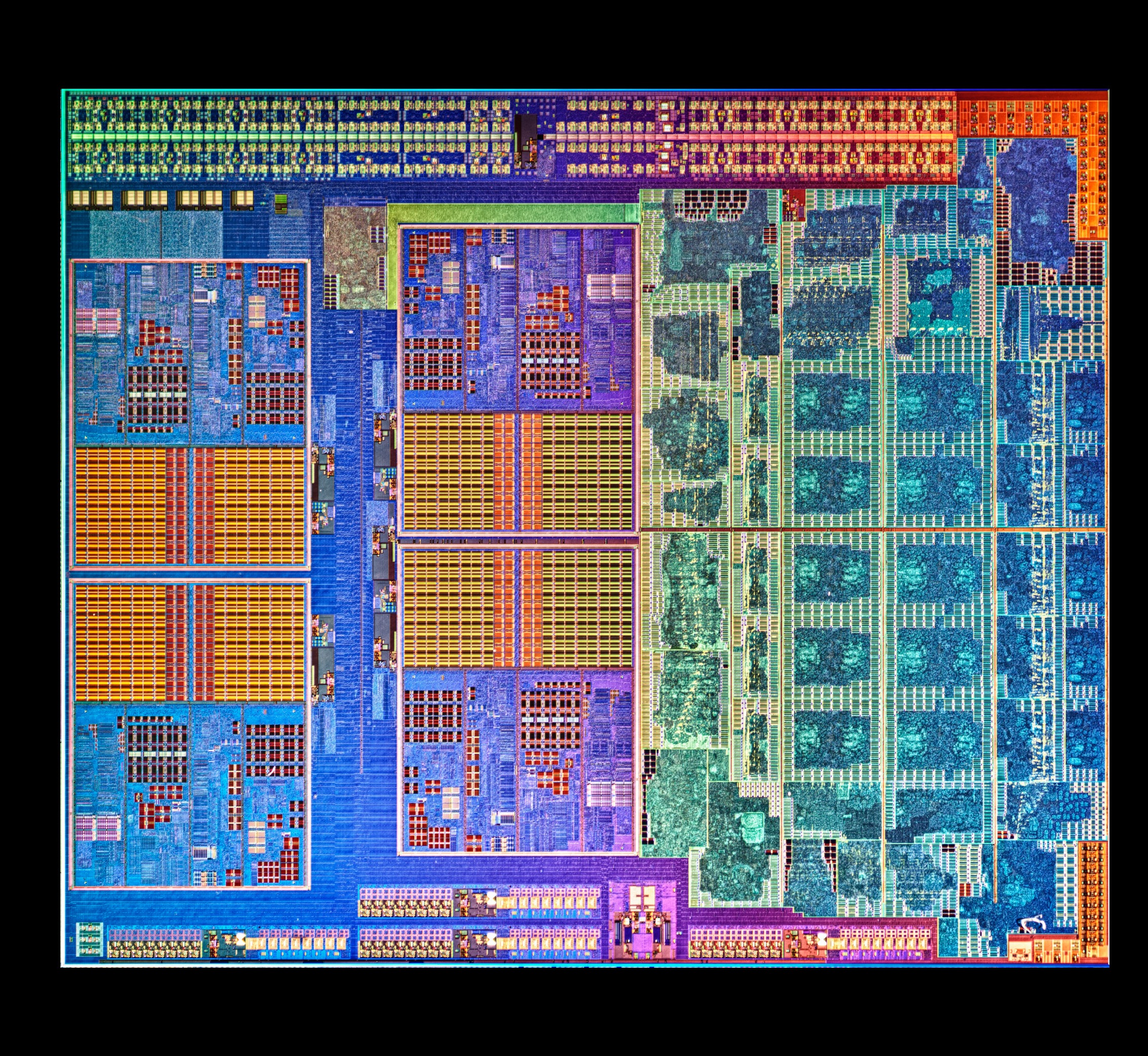
AMD sent along a high res shot of Kaveri's die. Armed with the same from the previous two generations, we can get a decent idea of the progression of AMD's APUs:
Llano, K10 Quad Core

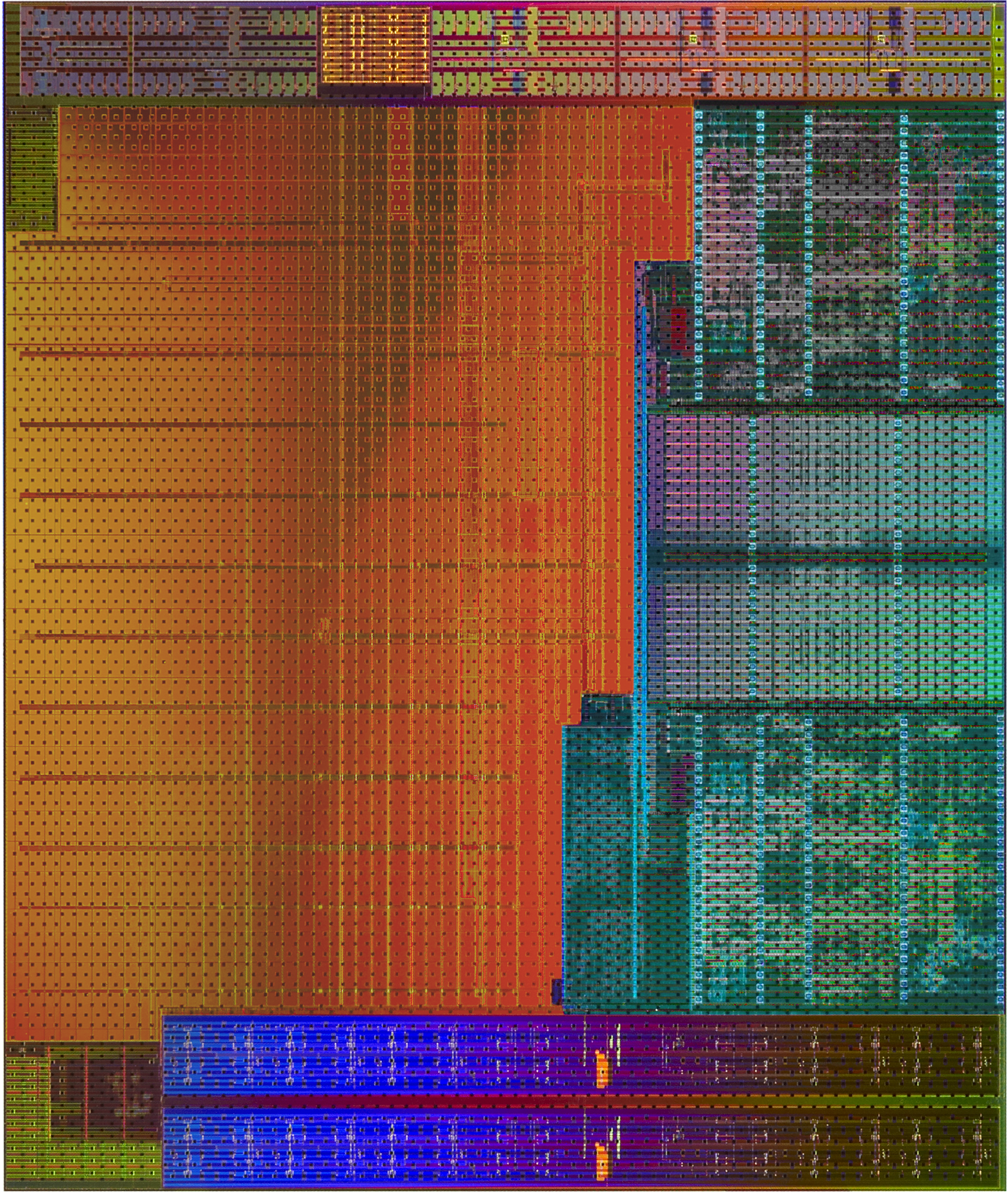
Trinity and Richland Die, with two Piledriver modules and processor graphics
Kaveri, two modules and processor graphics
Moving from Llano to Trinity, we have the reduction from a fully-fledged quad core system to the dual module layout AMD is keeping with its APU range. Moving from Richland to Kaveri is actually a bigger step than one might imagine:
| AMD APU Details | ||||
| Core Name | Llano | Trinity | Richland | Kaveri |
| Microarch | K10 | Piledriver | Piledriver | Steamroller |
| CPU Example | A8-3850 | A10-5800K | A10-6800K | A10-7850K |
| Threads | 4 | 4 | 4 | 4 |
| Cores | 4 | 2 | 2 | 2 |
| GPU | HD 6550 | HD 7660D | HD 8670D | R7 |
| GPU Arch | VLIW5 | VLIW4 | VLIW4 | GCN 1.1 |
| GPU Cores | 400 | 384 | 384 | 512 |
| Die size / mm2 | 228 | 246 | 246 | 245 |
| Transistors | 1.178 B | 1.303 B | 1.303 B | 2.41 B |
| Power | 100W | 100W | 100W | 95W |
| CPU MHz | 2900 | 3800 | 4100 | 3700 |
| CPU Turbo | N/A | 4200 | 4400 | 4000 |
| L1 Cache |
256KB C$ 256KB D$ |
128KB C$ 64KB D$ |
128KB C$ 64KB D$ |
192KB C$ 64KB D$ |
| L2 Cache | 4 x 1MB | 2 x 2 MB | 2 x 2 MB | 2 x 2 MB |
| Node | 32nm SOI | 32nm SOI | 32nm SOI | 28nm SHP |
| Memory | DDR-1866 | DDR-1866 | DDR-2133 | DDR-2133 |
Looking back at Llano and Trinity/Richland, it's very clear that AMD's APUs on GF's 32nm SOI process had a real issue with transistor density. The table below attempts to put everything in perspective but keep in mind that, outside of Intel, no one does a good job of documenting how they are counting (estimating) transistors. My only hope is AMD's transistor counting methods are consistent across CPU and GPU, although that alone may be wishful thinking:
| Transistor Density Comparison | ||||||||
| Manufacturing Process | Transistor Count | Die Size | Transistors per mm2 | |||||
| AMD Kaveri | GF 28nm SHP | 2.41B | 245 mm2 | 9.837M | ||||
| AMD Richland | GF 32nm SOI | 1.30B | 246 mm2 | 5.285M | ||||
| AMD Llano | GF 32nm SOI | 1.178B | 228 mm2 | 5.166M | ||||
| AMD Bonaire (R7 260X) | TSMC 28nm | 2.08B | 160 mm2 | 13.000M | ||||
| AMD Pitcairn (R7 270/270X) | TSMC 28nm | 2.80B | 212 mm2 | 13.209M | ||||
| AMD Vishera (FX-8350) | GF 32nm SOI | 1.2B | 315 mm2 | 3.810M | ||||
| Intel Haswell 4C (GT2) | Intel 22nm | 1.40B | 177 mm2 | 7.910M | ||||
| NVIDIA GK106 (GTX 660) | TSMC 28nm | 2.54B | 214 mm2 | 11.869M | ||||
If AMD is indeed counting the same way across APUs/GPUs, the move to Kaveri doesn't look all that extreme but rather a good point in between previous APUs and other AMD GCN GPUs. Compared to standalone CPU architectures from AMD, it's clear that the APUs are far more dense thanks to big portions of their die being occupied by a GPU.


380 Comments
View All Comments
LarsBars - Tuesday, January 14, 2014 - link
Thanks Ian / Rahul for the article, and thanks especially for having a page on the FX / server situation. I like to follow AMD news, and I trust AnandTech to be a reputable source that won't get emotional.I would love to know if you guys have any eta of any companies manufacturing 16GB DDR3 unbuffered non-ECC ram sticks, though.
SilthDraeth - Wednesday, January 15, 2014 - link
Going to go with a few other people here Ian, and Rahul, you guys point out that AMD wants to be able to play said games at 1080p at 30 frames per second.And yet, you didn't find a setting in your benchmark games that ran 30 fps, at 1080p, and then duplicated the settings for the other systems. I understand this will take a bit more work, but I would like to see it running Sleeping Dogs at 1080p, what settings where needed to hit 30fps, and then see what fps the rest of the systems hit at the same settings.
Can you please update this review with that information?
yottabit - Wednesday, January 15, 2014 - link
I'm very disappointed to see meaningful conclusions attempted to be drawn from benchmarks of 2-6 FPS in an Anandtech article. Saying things like "The Iris Pro really suffers in Sleeping Dogs at 1080p" is ridiculous when all the FPS are < 7. More useful info would have been about why the Iris pro gets hit harder... I'm assuming because the eDRAM is less and less effective at higher res and settings, and Intel has yet to solve the memory bandwidth issue. Obviously the Iris Pro has the raw GPU horsepower because it's able to keep up fine at the lower resolutions.I'm more impressed at how far Intel has come than AMD (who has historically enjoyed a large lead) in terms of iGPU tech. Thinking back to things like the GMA graphics and I'm very happy to see Intel where they are today.
yottabit - Wednesday, January 15, 2014 - link
It's also pretty bad to say things like a very easy to miss ambiguous line saying "Unfortunately due to various circumstances we do not have Iris Pro data for F1 2013" and then reference the same charts saying "none of the Intel integrated graphics solutions can keep up with AMD"duploxxx - Wednesday, January 15, 2014 - link
Obviously the Iris Pro has the raw GPU horsepower because it's able to keep up fine at the lower resolutions.you just proven yourself that you have no idea, since its the other way around.....
yottabit - Wednesday, January 15, 2014 - link
I doubt they were CPU bound in those instances, which seems to be what you seem to be implyingThere is a difference between being GPU bound and being GPU bound at certain settings and resolutions. I would assume the Iris Pro is going to suffer heavier from increases in resolution and detail because of its 128 MB eDRAM. If we could have seen increased quality testing at lower resolutions this would help affirm this. For instance shader intensive testing at a lower resolution...
yottabit - Wednesday, January 15, 2014 - link
Actually, we know they weren't CPU bound at lower resolutions, because the 6750 discrete card showed consistently higher results than the Iris Pro and AMD. If it were CPU bound you would think you'd see the same results with the 6750.What I was trying to say is that the Iris Pro is suffering disproportionately from some sort of scaling, and the article does little to compare what that is and what the advantage of the AMD is. Does the AMD have more shader power and that's why its able to scale better at high quality settings? Or does it have better memory bandwidth management and that's why its able to scale better at high resolutions? It's obviously scaling better somehow because the Iris Pro beats it in many benchmarks at low res but loses out at high res. Because the quality and resolution are coupled it's hard to learn what's going on. It might be a good system to use for Anandtech Bench but I would like to see testing data that is specific to the scope of the articles...
ericore - Wednesday, January 15, 2014 - link
This is the least impressive review I have ever seen on Anandtech; it's not horrible but its not anything near the usual fantastic mark I would give. I did like the bit on overclocking, but found the whole benchmark section completely designed without thought (or half-ass done), quite frankly you can remove the whole thing from the article. And where is the overclocked Kaveri in the benchmarks. First time, I've had to use other review sites.At 200$ cad, Kaveri will need a price cut if AMD expects this thing to sell well. No way that's worth 200$, 160 tops.
MrHorizontal - Wednesday, January 15, 2014 - link
HSA, hUMA and Mantle are all very interesting, but as has been pointed out many times, it's the API's that make or break a platform. On this note, there isn't a thing as a 'heterogenous' API. I can see situations where Mantle would help with Math acceleration in HPC contexts and also see where hUMA makes a lot of sense in desktop contexts. The HSA foundation has it spot on to standardise the instructions across all of these distinct technologies. In effect this would make HSAIL the 'holy grail' ISA. X86 would in effect be playing second fiddle to this. So, yes the real spur point is as mentioned - making the compilers, JITs and VMs aware of the stack and to use them when/if available. The issue is that there are only so many bytecodes a single program can support, so having the hardware speak the same language as an intermediary language like HSAIL means the bridge between hardware and software is made significantly easier. The proof as always is in the pudding, and it all depends on whether the design choices provided by HSAIL are good enough or not.You asked in the review whether it would be good to have a SoC with a much bigger GPU in it. The answer is yes and no. SoC's make a lot of sense to phone makers and heavily integrated high volume players, in particular, Apple. In fact, I'd be very surprised if Apple isn't talking to AMD about Kaveri and APU's generally. Because it's products like the iMac and Macmini that stand to benefit most from an APU - small computers driving enormous screens (if you realise that a Macmini is a firm favourite HTPC when driving a TV).
However, while there are isolated use cases such as Consoles, iMacs, Macminis and the like for a SoC like Kaveri, what I'd like to see is some more effort on making buses and interconnects between chips beefed up. The first and most obvious low hanging fruit to target it here is the memory bus, because SDRAM and it's DDR variants are getting a little long in the tooth. RAM is fast becoming a contention point *slowing down* applications, particularly in high throughput distributed contexts.
With AMD specifically, though, I'd like to see a (proprietary, if necessary) bus to allow all of the HSA, hUMA magic to happen betweeen a discrete CPU and GPU. In other words, I as an ISV or OEM can build a machine with a Jaguar CPU and a R9 card and employ the benefits of using a system heavily skewed to GPU usage (such a set up would be good for video walls, running 6-24 screens in a Single Large Surface Eyefinity set up). Alternatively, the bus, due to it's necessity to be quite wide should also be beefed up to access significantly more than 32GB of RAM. As a programmer, RAM is a massively limiting factor and I really could do with a high end laptop with 64-96GB RAM in it - why doesn't this exist? So buses. You saw how important HyperTransport was back in the day. Now we need a new one, a fully HSA compliant HyperTransport.
The bus within interconnected components in a machine is also only half the problem. The next problem after that is making a bus capable to leashing together multiple machines all working together as a heteregoneous cluster.
So yeah. SoCs are good, but there are simply too many use cases in business and industry where there is simply not enough justification to fabricate a custom SoC for a given task. Rather, it'd be far benefitial to provide all of these technologies in a modularised format, and ironically start transforming the PC to be more of a Transputer (Trannys were basically a machine with a super wide bus that you just plugged in modules. If you wanted more CPUs, plug a CPU module in. If you wanted graphics, storage etc, plug those in)
So I think AMD are definitely on the right track - but even they say it's only the first part of the puzzle to move to a post-X86 ISA:
- We need fully HSA-capable buses (first a HyperTransport-esque solution between discrete GPU and CPU, then a NUMA-esque solution to leash together clusters of machines)
- We need it to be an open spec with not just AMD, but Qualcomm, ARM and Intel (though they'll need to be strongarmed into it do lose control of the X86 golden goose, but I think even they realise this with their efforts in Iris and Knight's Landing)
- We need hardware to comply to industry standard bytecode, to meet the software people in the middle who all have to code to a specific specification
And with that, we'd truly have an end to the PC and X86 as a dominant architecture but the ISA actually targetting the bus and the set of capabilities of all hardware modules together rather than that of a specific CPU.
I'd also like to see an investigation or at least this question raised to AMD's engineers: why does Streamroller even need an FP unit at all? Can't the GPU effectively handle all FP work on the CPU side? Wouldn't it be cheaper/faster/better to put a fixed function emulation bridge to translate all X87 calls to GCN?
mikato - Wednesday, January 15, 2014 - link
For your last paragraph, I'm pretty sure something like that has been the idea since the beginning of Bulldozer/Piledriver/Steamroller/Excavator. It has an FP unit because they haven't gotten a way to move all that work to the GPU yet.