AMD at ISSCC 2015: Carrizo and Excavator Details
by Ian Cutress on February 23, 2015 7:45 PM EST
AMD is using the International Solid-State Circuits Conference this week to present a paper and announce some interesting developments regarding the next iteration of the Bulldozer architecture, codenamed ‘Excavator’, as well as other details regarding the CPU range that it will be placed in called ‘Carrizo’.
At the tail end of 2014 we reported on Carrizo and AMD’s announcement for its next generation of APUs, and more recently the discussion surrounding Carrizo not coming to desktop. In those announcements AMD revealed that Carrizo will be aimed at the laptop and notebook community first and foremost, a first for the company as previous APU designs have been aimed at both the desktop and mobile markets.
From a hardware standpoint, Carrizo will be combining a number of Excavator modules, AMD’s R-Series GCN GPUs, and the chipset/Fusion Controller Hub into a single package, bringing with it full HSA compatibility, TrueAudio, and ARM Trustzone compatibility. As with Kaveri before it, Carrizo will be built on Global Foundries’ 28nm Super High Performance (28SHP) node, making Carrizo a pure architecture upgrade without any manufacturing changes. Today’s ISSCC paper in turn builds on these revelations, showing some of the data from AMD’s internal silicon testing.

AMD’s presentation confirms that the new Excavator cores are low power optimized rather than desktop optimized. Support for Mantle and DirectX 12 should go without saying, and Dual Graphics support is something AMD has been working on for a number of generations. The next point is interesting from my perspective:
“Single-chip integration of the APU and the Southbridge onto a single die”
In our pre-briefing call, AMD confirmed that the Southbridge/FCH is no longer a separate chip, and is being moved on to the CPU from its previously separate package. In fact not only is the south bridge going to part of the CPU with Carrizo, but it's being fully integrated into the APU die itself. This is a first for AMD, and even Intel by comparison still uses two separate dies on the same package for their similar Broadwell-Y/U processors. As a result, AMD explained, this advances the Southbridge from the older 65nm/45nm processes to 28nm and 28SHP, reducing power consumption and operating voltage. It also allows the APU to accurately control power gating, further saving power, and reduces the length of HyperTransport interconnects between the APU and the I/O. On the flip side, it does move the soutb bridge's power consumption onto the APU, as well as the extra transistors it would otherwise occupy. This is explained in detail below.
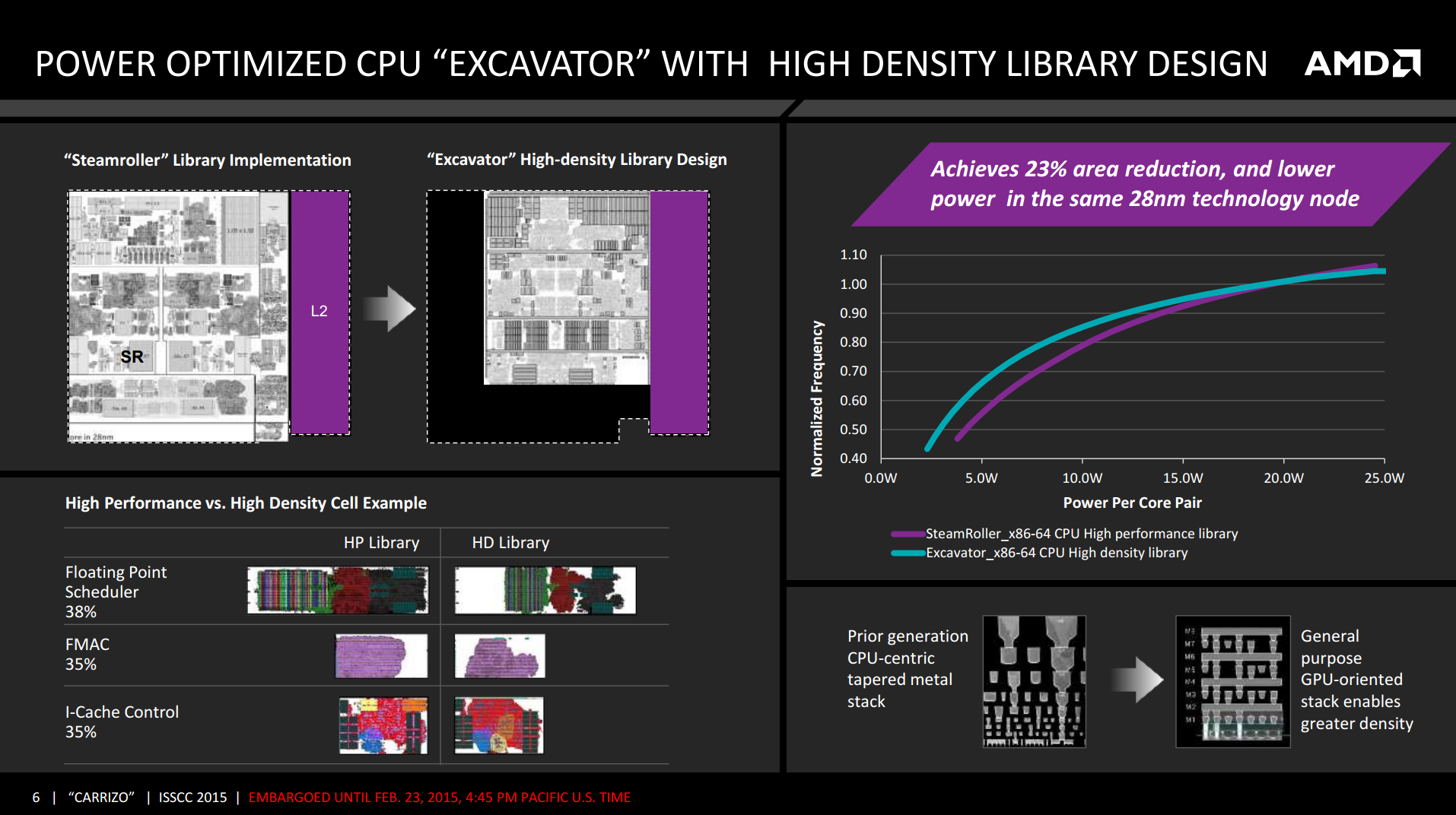
The key element to Excavator’s design is a reduction in die area. Fundamentally everything is the same in terms of operation compared to Kaveri, but the internal units such as the FP scheduler and cache control have been re-engineered to take up less room on the same 28nm SHP process node. It seems a little odd applying a ‘high-density’ design to a ‘high-performance’ process node, but AMD is stating that part of this has been driven by the GPU team sharing its experiences and knowledge of small, efficient die components with the CPU team, allowing the lessons learned there to benefit AMD's CPU designs. This is combined with a "GPU-oriented" design stack on the CPU, which AMD is showing provides significant power savings at the same frequency, or higher frequency at the same power.
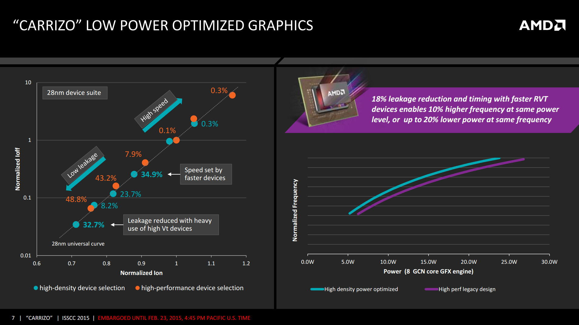
The high density, power optimized design also plays a role in the GPU segment of Carrizo, offering lower leakage at high voltages as well as allowing a full 8 GCN core design at 20W. This is an improvement from Kaveri, which due to power consumption only allowed a 6 GCN design at the same power without compromising performance.
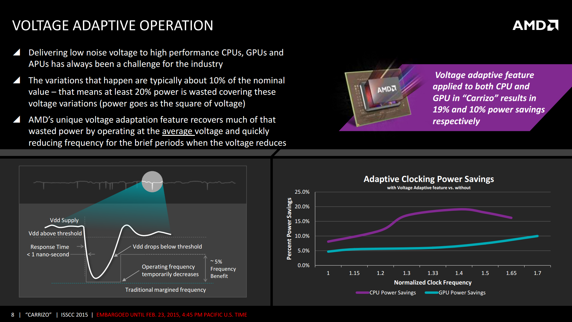
AMD revealed Voltage Adaptive Operation back with Kaveri, and it makes a reappearance in Carrizo with its next iteration. The principle here is that with a high noise line, the excess voltage will cause power to rise. If the system reduces the frequency of the CPU during high noise/voltage segments - as power is proportional to voltage squared - power consumption will be reduced and then frequency can be restored when noise returns to normal. This happens inside the CPU over nanoseconds, resulting in no serious performance loss but it helps keep the power consumption of the APU down. In the case of Carrizo, AMD is quoting a 10-20% reduction in power consumption versus what a theoretical Carrizo would look like without this technology.
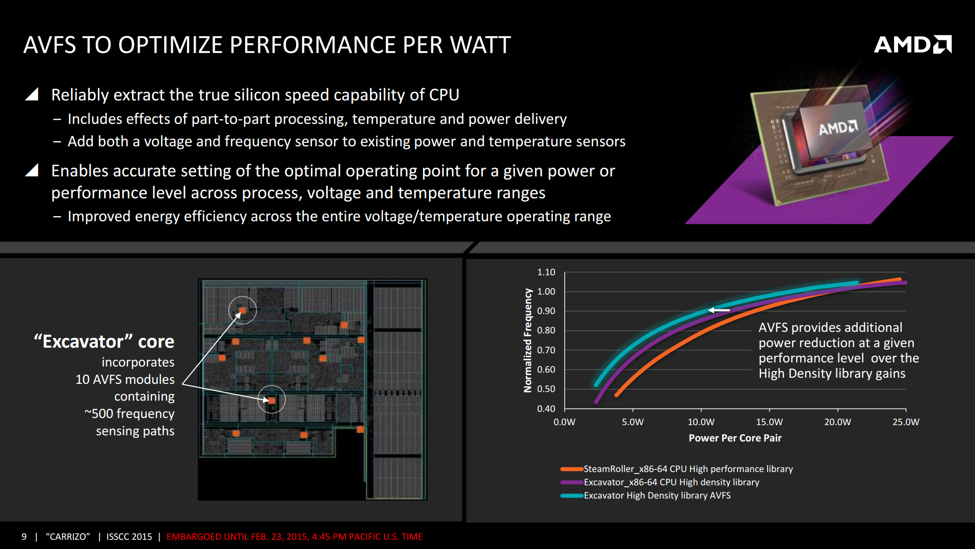
Another new addition to Excavator comes in the form of Adaptive Voltage-Frequency Scaling modules. Carrizo uses 10 in each Excavator ‘core’, and these modules can adjust the frequency and voltage of individual components depending on power requirements, temperature and other external factors in order to improve either performance, power consumption, or efficiency. With this in mind, AMD is claiming a 29% frequency increase at 10W, or if frequency is held constant then there is a 40-50% power decrease at the same 10W. At 20W, as the graph shows, there is almost no difference between the two, indicating that Excavator is truly built for lower TDP devices.
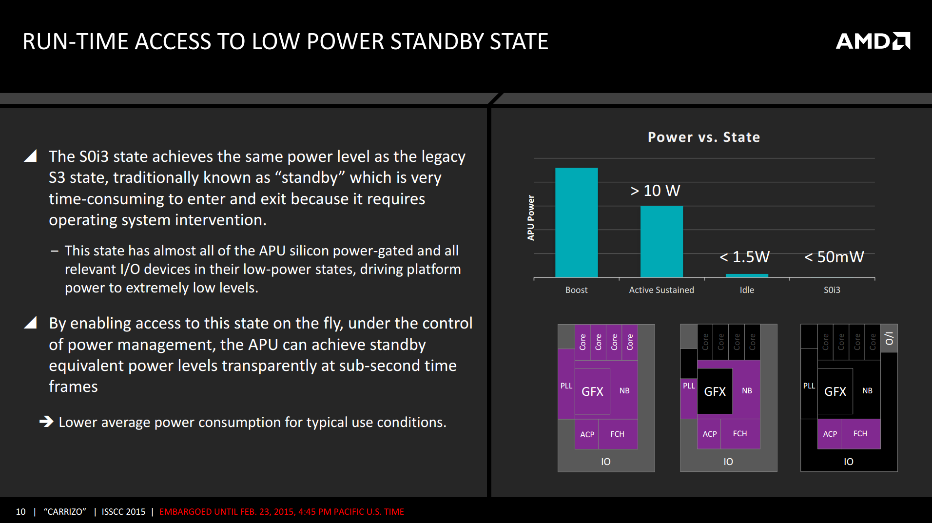
AMD is also presenting news on improvements to their ability to quickly enter and exit sleep states. With Excavator, AMD can now go from a sub-50mW S0i3 state to an active state in under a second. This should allow Carrizo devices to quickly reach and better sustain near-standby power levels, improving idle and low-load power consumption. As shown in the slide, at the S0i3 state only the ACP, PCH, and a small I/O segment are still active, while the rest of the device is completely power gated.
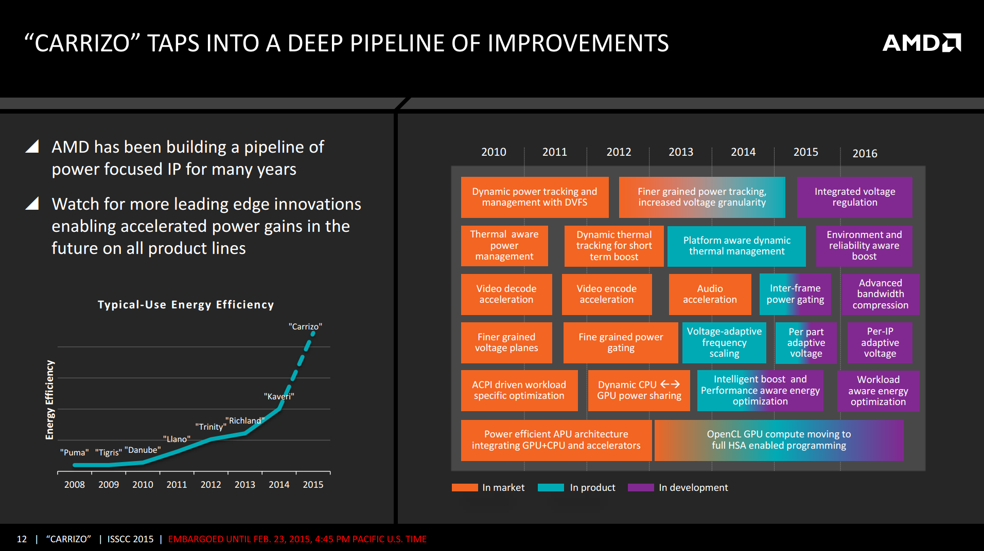
Meanwhile AMD is also once again showing off their technology timeline to illustrate their progress in implementing new technologies over the years. We confirmed that an interesting feature, inter-frame power gating, is active in Carrizo. This in a nutshell allows the GPU to go to a low frequency mode when the frame buffers are full. Though only a few milliseconds of power savings per instance, over time this can add up to larger increases battery life.
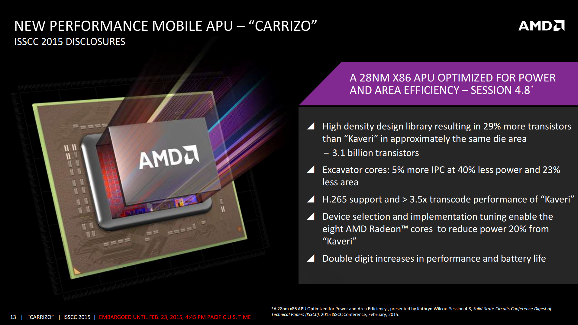
Wrapping up the hardware aspects of their ISSCC presentation, AMD is also disclosing the die size and transistor counts for Carrizo. Whereas Kaveri weighed in at 2.3 billion transistors in a 245mm2 die, Carrizo will come in at a much larger 3.1 billion transistors in a 250mm2 die. This a significant increase in transistor density for AMD, with Carrizo packing in 29% more transistors for only a marginal increase in die size. Though AMD is not explaining where all of the transistor increases come from at this time, part of the increase comes from the Southbridge/FCH being moved on-die, which AMD tells us will take up 5.5% of Carrizo's die. As for the Excavator cores themselves, AMD is starting that they consume 40% less power and take up 23% less die area, thanks to the combination of transistor density improvements, AVFS technology, and bringing the FCH on-die.
Moving on, although AMD's ISSCC presentation is not going to be diving deep into the Excavator architecture, AMD is claiming that Excavator will also bring with it a 5% IPC boost. We understand that this increase in IPC comes from a doubling of the L1 data cache from 64KB to 128KB, as well as further payoffs from the power improvements. Meanwhile on the fixed-function side of matters, Carrizo will be introducing a full H.265 hardware decoder. This is the first AMD part (CPU or GPU) to offer any kind of hardware support for H.265 decoding, and in the process it will be the first x86 CPU/APU to offer full hardware decode capabilities, as Intel still relies on a hybrid decode approach at this time.
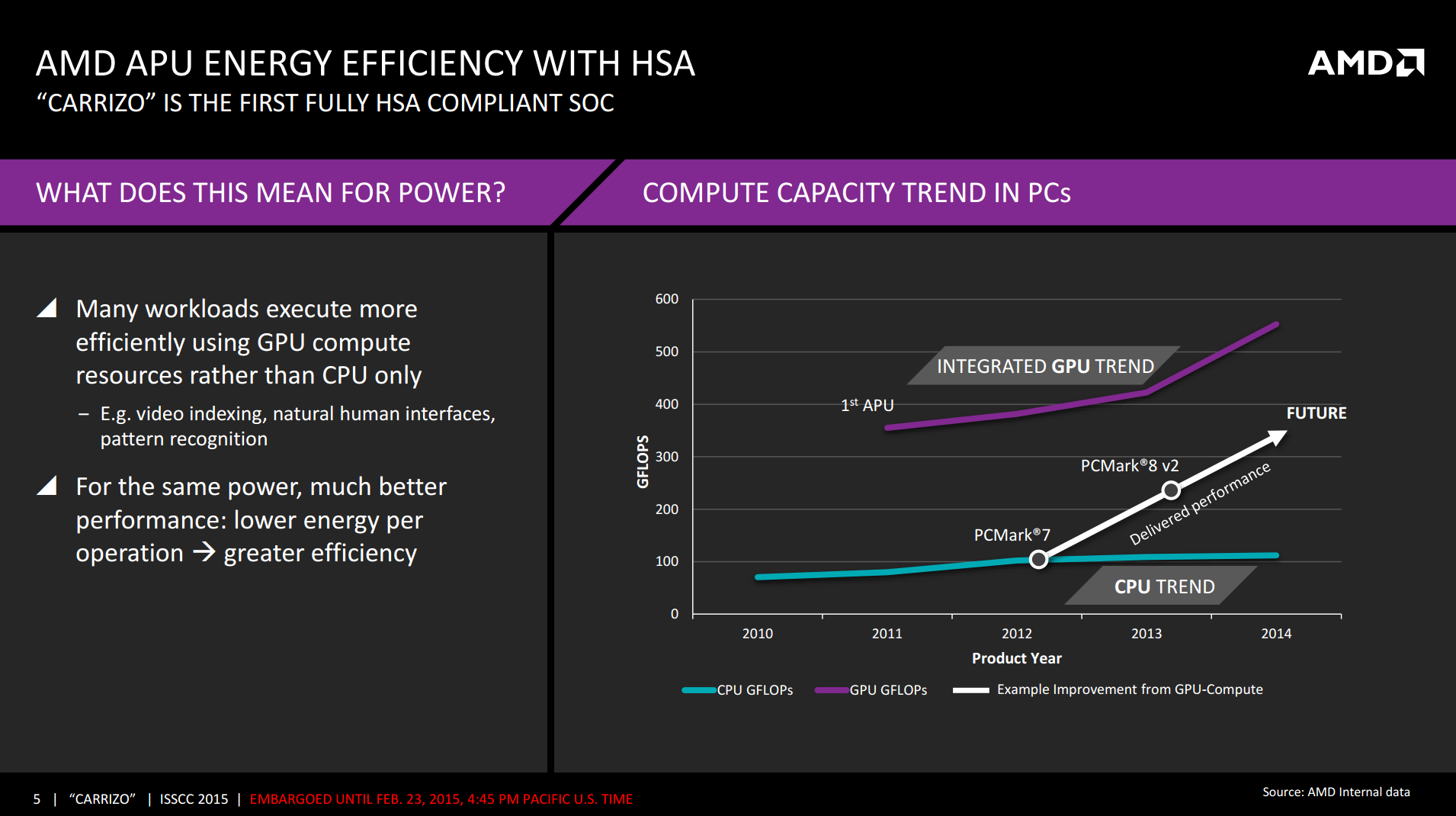
Finally, AMD is also rolling out some new Heterogeneous System Architecture (HSA) functionality as part of Carrizo. HSA is seen as one of the next key factors in personal computing over the next decade. We have seen an almost ubiquitous shift in recent years towards almost every consumer processor having on-die graphics, and the ability to optimize a workload for each part of the system improves the experience. AMD has been riding this wave, announcing Kaveri as ‘HSA Ready’ and now Carrizo as ‘HSA Compliant’, fully adhering to HSA 1.0 specifications. At the moment the biggest benchmark showing off this power is PCMark, something AMD likes to promote. With regards the difference between HSA Ready and Compliant, I asked AMD what made Kaveri different in that regard. The answer was straightforward enough: Carrizo is able to perform GPU context switching, allowing a GPU state-save and state-restore, something Kaveri is unable to do and offering a solid hint that Carrizo's GPU is based on AMD's GCN 1.2 architecture.
Wrapping things up, the combination of a 5% IPC boost and 40% power savings means that AMD has a range of options for Carrizo parts, picking between increased clockspeeds at the same power levels or holding clockspeeds constant for a larger battery life gain. We expect that actual retail parts will be somewhere in the middle, as the graphs in the slides indicate that best efficiency occurs around the 10W scenario.
We did ask about absolute design numbers regarding battery life, processor frequencies and time to market. As expected, AMD is keeping its cards close to its chest, especially in a more academic environment such as ISSCC. At this point in time we were told that Carrizo is expected to come to market within Q2. With Computex taking place towards the end of Q2, this should mean that a number of Carrizo devices will either be on the market or at least on display for us to examine.


79 Comments
View All Comments
yannigr2 - Tuesday, February 24, 2015 - link
The bad thing is that this chip will battle against Intel's contra revenue, and there AMD has almost zero chances.zodiacfml - Tuesday, February 24, 2015 - link
Right. That's with Bay Trail devices. For bigger devices such as notebooks with Carrizo where I expect it to be used more, it might end up more expensive to an Intel Celeron with the same performance with a slightly higher power consumption.jabber - Tuesday, February 24, 2015 - link
Why are they even bothering? None of these chip will ever appear in a decent laptop worth more than $300. Where are all the value add and feature packed AMD APU laptops with 1080P IPS screens, 256GB SSD, 8GB Ram, blu-ray etc. etc. Yes that's right...they never existed, never will!Scandal really.
Valis - Tuesday, February 24, 2015 - link
Yeah that's true, I would never buy or recommend a note/lap with 1366x768, these days, to anyone, ever. No matter the price, it's just so 2006 (or what they say).MrSpadge - Tuesday, February 24, 2015 - link
So they have significantly better energy efficiency and die area savings on top of any savings from moving 32 nm to 28 nm. Yet they don't use this to produce some many-module chips for their dekstop & server platforms. With this technology they could probably offer 6 modules in cheaper than their current 4 module chips. Single threaded performance still won't be great, but for some markets that's OK. That they're not doing this shows just how badly their financial situation is - they focus heavily on whatever they they can still sell in half-decent quantities and try nothing else. If this makes them survive - well, so be it. It's just sad to see them develop these optimization, yet not using them across most of their product range.Pissedoffyouth - Tuesday, February 24, 2015 - link
I agree, how about they release these @ 65w and 95w for desktop APU's, and 125w AM3 drop ins. With 30% more frequency at same power they could release 4.5ghz 8 cores or something?firex123 - Tuesday, February 24, 2015 - link
There's a graph that shows that the power savings due to high density design effectively end at 20W and beyond... so, energy-efficient Carrizo chips are pretty much geared towards lower TDP form factors.testbug00 - Thursday, February 26, 2015 - link
20W PER MODULE. So, in theory, a 65W SKU is perfectly reasonable. 40W for the CPU and 25W for the GPU + MISCUrizane - Wednesday, February 25, 2015 - link
Making something wide (greater than 4 modules) that can run highly multithreaded software is in direct opposition to AMD's stance on HSA.Oxford Guy - Tuesday, February 24, 2015 - link
They are hoping to build greater enthusiasm for Zen by having a much more massive jump in improvement. Of course, Intel has been delaying Skylake forever so it will be able to drop 10nm or whatever on AMD as soon as Zen is released.