Analyzing Intel-Micron 3D XPoint: The Next Generation Non-Volatile Memory
by Kristian Vättö, Ian Cutress & Ryan Smith on July 31, 2015 11:00 AM EST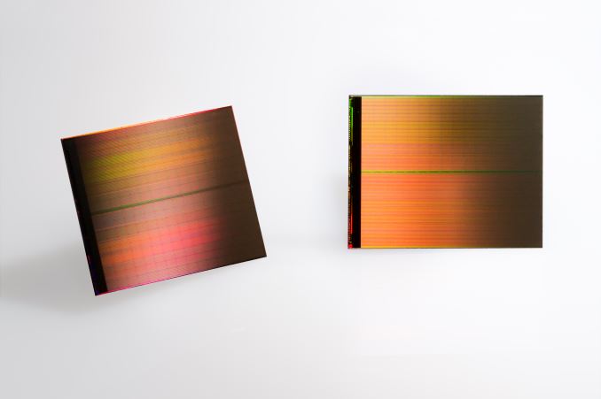
The current mainstream memory technologies, namely DRAM (quick memory accessed by the processor) and NAND (solid-state storage), have been around for decades. While the cell designs have evolved over the years to allow scaling to 20nm and below, the fundamental physics behind DRAM and NAND operation haven't changed a bit and both technologies have their unique technological limitations. DRAM offers nanosecond-level latency and unlimited endurance, but this comes at the cost of large cell size, cell volatility, and power consumption. Since DRAM cells need to be constantly refreshed, the cells don't retain data in an off state, requiring quite a bit of power and making DRAM unsuitable for permanent storage. NAND, on the other hand, has much higher latency (especially write operations) and has a limited number of write cycles, but the cells are non-volatile and the structure is much more efficient, enabling low cost and suitability for storage.
Combining DRAM and NAND at the system-level architecture provides the best of both worlds, which is why modern computers use DRAM as a memory/cache and NAND for storage. However, there's still a latency and capacity gap between DRAM and NAND, so the question arises: what if you were to combine the best of DRAM and NAND at the silicon level? The mission of next generation memory technology across the industry has been to develop a new type of memory that provides low latency and high endurance while offering a small and scalable cell size.
We have seen numerous startups, such as Crossbar and Nantero, discuss and demonstrate their next generation memory technologies, but we have yet to see the established DRAM and NAND vendors come out with their solutions. Intel and Micron are here to change that with the announcement of their new 3D XPoint (Cross Point) non-volatile memory technology this week.
First and foremost, Intel and Micron are making it clear that they are not positioning 3D XPoint as a replacement technology for either NAND or DRAM, and in that scale it has been talked about more in its applications nearer NAND than DRAM. It's supposed to complement both and provide a technology that sits in between the two by filling the latency and cost gap exists between DRAM and NAND. Basically, 3D XPoint is a new tier in the computer architecture because it can be used as either slower, non-volitile memory or much faster storage.
| DRAM | 3D XPoint | NAND | |
| Endurance (P/E Cycles) | 10^15 | 10^7 | 10^3 |
| Read Latency | Nanoseconds | 10s of Nanoseconds | ~100 Microseconds |
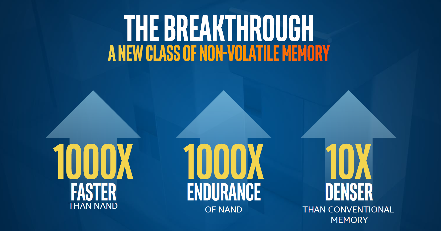
Intel and Micron are claiming that 3D XPoint provides up to a thousand times higher endurance than NAND. Assuming that the numbers are relative to modern (15-20nm) MLC NAND, the endurance should be in the order of a few million P/E cycles; though the marketing materials are claiming up to tens of millions of write cycles. If we assume 3 million write cycles (1000x of what modern MLC has), a 256GB 3D XPoint based drive would have a total write endurance of 768 petabytes. That's equivalent to 420TB per day for five years, or 4.9GB per second. For storage applications that currently rely on NAND, 3D XPoint will eliminate any potential endurance concerns, but it's not durable enough to challenge DRAM in that front since DRAM endurance is essentially infinite. Whether 3D XPoint provides enough endurance to replace DRAM ultimately depends on the application, but especially in certain enterprise workloads there's a need for DRAM.
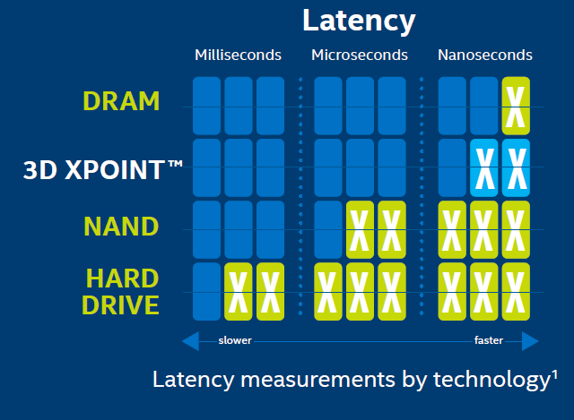
3D XPoint latency should be in the order of 10s of nanoseconds, but the companies didn't specify whether this is read or write latency. Judging by the graphs provided by Intel, it seems to be read latency because NAND write latency would measured in milliseconds (typically 1-2ms for a full page write), whereas the graph puts NAND latency at tens of microseconds that is in line with NAND read latency. Write latency is likely higher than that, probably at least 100s of nanoseconds or even a few microseconds given Intel and Micron's claims of "up to 1000x faster than NAND", but what complicates things is that 3D XPoint is accessible at the bit-level whereas NAND is page-level, so comparing the latency of the two without extended context is quite difficult. In any case, 3D XPoint performance should be closer to DRAM than NAND, but since Intel and Micron aren't discussing any specific latencies yet it's too early to make any final conclusions.
Meanwhile unlike many next generation memory technologies out there at the moment, 3D XPoint is the furthest along and doesn't only exist on paper or in a lab. Intel and Micron are currently sampling the first generation die that is being produced at the companies' jointly owned fab in Lehi, Utah. The die is 128Gbit (16GB) in capacity, whereas the products that startup memory companies have in production are in the order of dozens of megabytes. The die is built on a 20nm node and consists of two layers, and in the future scaling will happen through both lithography shrinks and by increasing the number of layers.
The Utah fab has been producing 20nm NAND for now since Intel didn't invest on the 16nm shrink and all initial 3D NAND production will take place in Micron's Singapore fab, but it's unclear whether the full fab with its 20,000 wafers per month capacity will be dedicated to 3D XPoint from now on. My guess would be that 3D XPoint will gradually take over the full wafer capacity in Utah depending on how the market reacts to the new technology and how high demand Intel and Micron are seeing. 3D XPoint does require some new equipment for manufacturing since 3D XPoint deals with a whole new set of materials, but Intel and Micron said that the transition is quite similar to a new NAND node and allows some of the existing equipment to be used.
The companies aren't quoting any price per gigabyte yet, but since the whole function of 3D XPoint is to fill the gap between DRAM and NAND, it will also be priced accordingly. A quick look at NewEgg puts DRAM pricing at approximately $5-6 per gigabyte, whereas the high-end enterprise SSDs are in the range of $2-3. While client SSDs can be had for as low as $0.35, they aren't really a fair comparison because at least initially 3D XPoint will be aimed for enterprise applications. My educated guess is that the first 3D XPoint based products will be priced at about $4 per gigabyte, possibly even slightly lower depending on how DRAM and NAND pricess fall within a year.


80 Comments
View All Comments
Kristian Vättö - Monday, August 3, 2015 - link
That's a good point and admittedly something I didn't think about. I would assume 3D XPoint is more robust than NAND given the higher performance and endurance, but Intel/Micron declined to talk about any failure mechanisms, so at this point it's hard to say how robust the technology is.Nilth - Sunday, August 2, 2015 - link
Well, I really hope it won't take 10 years to see this technology at the consumer level.dotpex - Monday, August 3, 2015 - link
From Micron site https://www.micron.com/about/innovations/3d-xpoint..."Memory cells are accessed and written or read by varying the amount of voltage sent to each selector. This eliminates the need for transistors, increasing capacity and reducing cost."
...but 3d xpoint will be expensive, more like $10 per gigabyte.
Adam Bise - Friday, August 7, 2015 - link
"First and foremost, Intel and Micron are making it clear that they are not positioning 3D XPoint as a replacement technology for either NAND or DRAM"I wonder if this is because they would rather create a new market than replace an existing one.
hans_ober - Saturday, August 8, 2015 - link
@Ian. PhD Chem was useful! :)Ian Cutress - Monday, September 28, 2015 - link
Yiss :)duartix - Monday, August 10, 2015 - link
I see two immediate consumer usages:a) Instant Go To / Wake From deep hibernation
b) Scratch disks
MRFS - Monday, August 24, 2015 - link
With proper UEFI/BIOS support, one feature we proposed in a Provisional Patent Application was a "Format RAM" option prior to running Windows Setup. This would format RAM as an NTFS C: partition into which Windows software would be freshly installed. For comparison purposes, imagine a ramdisk in the upper 32-to-64GB of a large 1-to-2 TB DRAM subsystem, in a manner similar to how SuperSpeed's RamDisk Plus allocates RAM addresses. Then, imagine that all 2 TB consist of Non-Volatile DIMMs. I can see this one feature enabling very rapid RESTARTS, even cold RESTARTS after a full power-down (for maintenance). If the UEFI/BIOS is told that the OS is already memory-resident, this one change radically improves the speed with which a routine STARTUP occurs i.e. currently a STARTUP must load all OS software from a storage subsystem into RAM. If that OS software is already loaded into RAM, that "loading" is mostly eliminated under these new assumptions. Moreover, mounting Optane on the 2.5" form factor should free designers to consider more aggressive overclocking of the data cables connecting motherboards to those 2.5" drives: just work backwards from PCIe 4.0's 16GHz clock and 128b/130b jumbo frame. It's possible that Optane will be fast enough to justify data cables that also oscillate at 16GHz, increasing to 32GHz with predictable success. Assuming x4 NVMe lanes at PCIe 4.0, then 4 lanes @ (16G / 8.125) ~= 4 lanes @ 2GB/s ~= 8 GB/s raw bandwidth per 2.5" device. Modern G.Skill DDR4 easily exceeds 25GB/s raw bandwidth. Thus, Optane should allow "overclocked" data cables to achieve blistering NVMe storage performance with JBOD devices, and even higher performance with RAID-0 arrays.FutureCTO - Tuesday, November 15, 2016 - link
I don't know, is it possible to have an educated guess on this? Back in the PS2 days, before the PS3, i was @0zyx on forum or few, talking about NASA RAM, magnet donuts on a metal grid of wires, insisting why don't we do this with memory today? The electricity crosses and creates a charge or reads the charge. This is the RAM of the first space computer. ~ I was made confident by believing this is what AMD "Mirror Bit" Memory was working towards before it flat out evaporated from the internet? Same happened to 48Bit Intel "Iranium" processors with 16cores. Still look in books from time to time, hoping an old edition of hardware lists with intel spy cpu, will confirm the internet is a BlackHole. Not to go Ellery Hale, with being one of those to store curious science bits no one is using, and everyone should be clamoring to own some day. ~ I check the metal recycling at the city dump for computer servers and extra high grade tower cases for my own builds, at least a parts from the towers anyways. ~ Twitter @0zyx ~ either way this is the memory design from the first NASA space capsule to carry people into space, except larger than 1 kilobyte. It may have been 512Bytes back then, not sure what sort of grid that is?FutureCTO - Tuesday, November 15, 2016 - link
educated guess on price? ~ To me it is simpler to make, and faster to verify trace integrity.