GlobalFoundries Plans to Expand Dresden and NY Fabs in Anticipation of 28/22nm
by Anand Lal Shimpi on May 31, 2010 11:44 PM EST- Posted in
- Trade Shows
- CPUs
- GlobalFoundries
Only a year has passed since AMD officially spun off its manufacturing division with the help of ATIC. The resulting GlobalFoundries have been busy getting its ducks in a row in preparation for inevitable battle with TSMC. It started with construction of Fab 8 (formerly GF Fab 2) in Saratoga County, NY due for revenue production in 2012. Today GF is announcing plans to expand Fab 8 before its completion and an expansion to Fab 1 (formerly AMD Fab 30/36) in Dresden.
Global also announced initial plans to create a similar cluster of fabs in Abu Dhabi. These clusters are placed on a site that can house three manufacturing modules, similar to what’s being expanded at Dresden and being built in Saratoga County. Given that GlobalFoundries’ majority shareholder is ATIC, an investment arm of the government of Abu Dhabi, the next location for fab expansion makes perfect sense.

At the end of last year, ATIC announced that it would acquire Chartered Semiconductor for $3.9 billion. The acquisition gave GlobalFoundries a 300mm fab in Singapore. The move wasn’t about taking out a competitor, but rather acquiring a customer base on aging manufacturing processes and giving them the option of migrating to smaller transistor geometries, something Chartered didn’t have the roadmap to do. A very smart move on GlobalFoundries’ part. To make room for the planned growth we have the aforementioned expansions at Fab 1 and Fab 8.
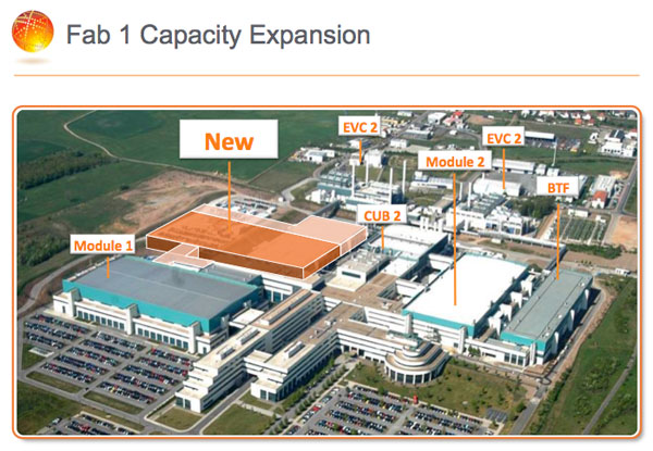
Fab 1 will get a new facility that can manufacture 45/40/28nm wafers and take Dresden’s total maximum output from 50,000 wafers per month to 80,000. The first production from this expansion will ship in 2011. We can also expect to see initial 22nm development done here, with Fab 1 eventually shifting to 22nm production over time.
Fab 8’s clean room will grow another 40% by the time it’s done. The original plans for Fab 8 targeted 35,000 wafer starts per month, but with the expansion we’re looking at a maximum of 60,000 with additional equipment.
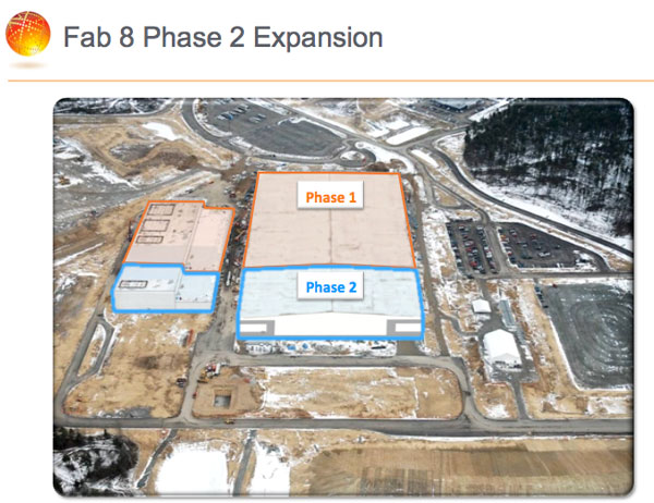
It’s not all good news though. Fab 8 is still expected to ship revenue generating wafers starting in 2012, but volume production won’t happen until 2013. Thankfully ATIC has very deep pockets.
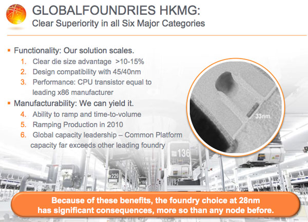
GlobalFoundries has often mentioned to me that if it had a customer willing to pay for it, it could offer transistor size and performance on par with Intel. In the past, AMD simply hadn’t been willing (or able) to pay for it. The 3rd bullet point on the slide below seems to make that same statement publicly.
A good AMD design coupled with a good process from GF could do some damage. Will Bulldozer be that design? It’s far too early to tell. Personally I’m more interested in seeing what a GPU manufactured at GlobalFoundries would look like.


11 Comments
View All Comments
Sahrin - Tuesday, June 1, 2010 - link
see what a really aggressive ARM design could do on a cutting-edge process. I get the impression that one of the things holding ARM back from being competitive (with Moorestown, forget mainstream x86) is that it not only constrained by the power requirements, but even further by the aged process nodes that it is fabbed on by less experienced foundries.As for AMD; this would only be a win. As you point out, it's only AMD's unwillingness to pay to 'be like Intel' that holds them back. The entire notion is that you 'spread R&D across many customers' and improve the quality of your top-end processes (which benefits first and foremost AMD).
I imagine the game console manufacturers will be all over GF when the time for renewal comes. Intel-like volume, QC, Process tech? Sold.
And the final piece is nVidia. With the way GF is shaping up (and the comparatively incompetent manner in which TSMC is handling their process transitions), I don't see how nVidia can avoid setting up shop with GF. TSMC needs to start getting serious about process development, or they're going to lose every single high-performance (read: high-margin) customer they have to GF.
RedemptionAD - Tuesday, June 1, 2010 - link
Except that GF is kinda part of AMD and the ATI graphics cards may prove a limit, but that depends on the contract limitations.Zoomer - Wednesday, June 2, 2010 - link
I'd say it'll probably be nVidia that would be reluctant. It's not like having early access to your competitior's general design relatively early on is a bad thing. :pyanfei - Sunday, July 25, 2010 - link
======= http://www.fashionshoppong.us=======veri745 - Tuesday, June 1, 2010 - link
"A good AMD design coupled with a good process from GF could do some damage. Will Bulldozer be that design? It’s far too early to tell."It obviously won't be Bulldozer unless you're talking about the already existing GF 32nm process. GF28nm is going to be bulk only, and it'll be an iteration of bulldozer that appears on 22nm.
HobHayward - Tuesday, June 1, 2010 - link
"The acquisition gave GlobalFoundries a 300mm fab in Singapore."Pretty sure you meant 300nm... :P
LuxFestinus - Tuesday, June 1, 2010 - link
@HobHaywardQuote:
"Pretty sure you meant 300nm... :P"
Well I am absolutely sure that they meant 300mm as in wafer size. Look it up if you don't believe me. 300mm wafer sizes are cheaper in the long run with economies of scale over 200mm wafers. This is why this is important.
Penti - Tuesday, June 1, 2010 - link
That site was also already at AMD APM tech/process and was already manufacturing AMD processors since years ago.Global Foundries are some years of at manufacturing GPUs though. AMDs chipsets and GPUs are still manufactured at TSMC because it's designed to be fabbed there, are at the right process nodes already, has lines, tools and all setup already and are at the cutting edge for those products and AMD needs most of GF's capacity for processors, obviously they fab a lot of other things now too. In two or three years though they might manufacture GPUs and such. When it comes to consoles they use IBM Power processors atm and those are generally fabbed by IBM themselves in New York not that far from where AMD planned there factory, the CELL are fabbed by "STI" in Japan though. But the tech for that factory is supplied by IBM and Toshiba. IBM tried to manufacture GPUs in the past tough. They don't have a lot to chose from, it's basically Power and IBM or x86 and Intel. ARM and MIPS are reserved to the portable consoles today. Next gen GPUs are of course limited to AMD/ATi and NVIDIA atm. Where they are fabbed are another matter though. The Singapore site (Former CSM) is at 45nm atm. But can also fab at a larger process. ATi/AMD is at 40nm at TSMC (or a half node). It's also designed to be fabbed there. They don't just manufacture for AMD there at the Singapore plant because for the Chartered legacy. They build in order to be able to fab for others now though, and other products like GPUs, but that won't happen till 28nm I would think.
veri745 - Wednesday, June 2, 2010 - link
300mm is the actual diameter of the wafer, not the size of the process that goes on it.dew111 - Tuesday, June 8, 2010 - link
"gave GlobalFoundries a 300mm fab in Singapore. The move wasn’t about taking out a competitor, but rather acquiring a customer base on aging manufacturing processes and giving them the option of migrating to smaller transistor geometries"He did mean nm, the passage refers to an aging 300nm process, and customers which can upgrade to newer ones. The passage also refers to the 300mm value as a transistor geometry size, which clearly indicates that he meant nm. LuxFestinus is correct in that 300mm wafers are better than 200mm, but GF already had 300mm wafer production in Dresden.