Analyzing Intel-Micron 3D XPoint: The Next Generation Non-Volatile Memory
by Kristian Vättö, Ian Cutress & Ryan Smith on July 31, 2015 11:00 AM ESTEstimating 3D XPoint Die Size
By now most of you probably know that I'm a sucker for die sizes and since this is information that the DRAM and NAND vendors are unwilling to share, I've gone as far as developing my own method for estimating the die size (well, it's really just primary school geometry, so I can't take too much credit for it). Die size is the key factor in determining cost efficiency because it directly relates to the number of gigabytes each wafer yields and thus it's a vital metric for comparing different technologies and process nodes.
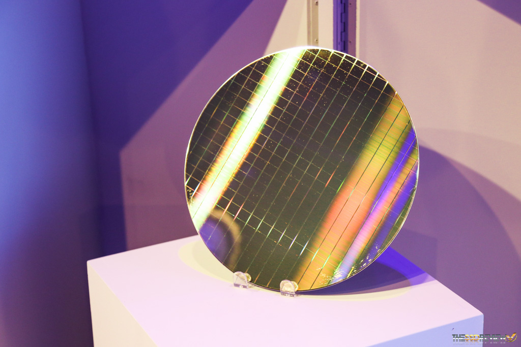
I'm borrowing the above picture from The SSD Review because to be honest my wafer photos (and photos in general) are quite horrible and wafers are far from being the easiest object given all the reflections. Sean is a professional photographer, so he managed to grab this clear and beautiful photo of the production 3D XPoint wafer Intel and Micron had on display, making it easy to estimate the die size.
I calculated 18 dies horizontally and 22 vertically, which yields 227mm^2 with a normal 300mm wafer. When taking die cuts (i.e. the space between dies) into account, we should be looking at 210-220mm^2. Array efficiency is about 90%, which is much higher than planar NAND because most of the peripheral circuitry lies underneath the memory array.
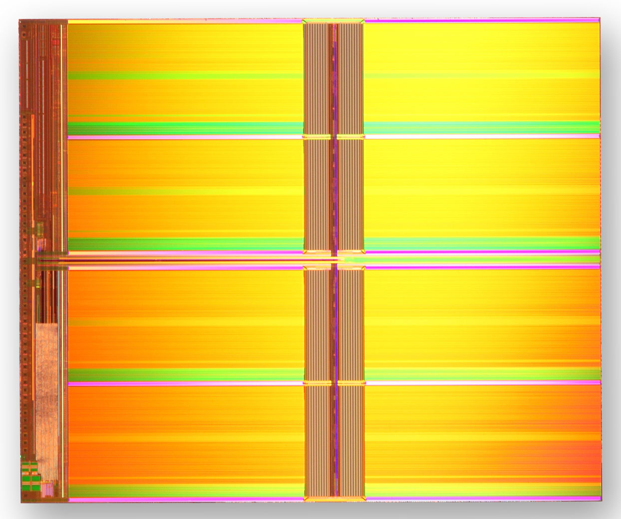
IMFT 20nm 128Gbit MLC NAND die
For comparison, Intel-Micron's 20nm 128Gbit MLC NAND die measures 202mm^2 and has array efficiency of ~75%. From that we can calculate that the 128Gbit memory array in 3D XPoint takes about 190mm^2, while a similar capacity planar NAND array measures ~150mm^2 (since the 128Gbit 3D XPoint die consists of two layers and 128Gbit MLC NAND die stores two bits per cell, the number of layers and bits stored per cell cancel out). It seems like NAND is denser (about 20-25%) from a memory array perspective given a fixed feature size (i.e. lithography), but at this point it's hard to say whether this is due to the cell design itself or something else. Connecting layers of wordlines and bitlines to the intermetal layers likely takes some extra area compared to a 2D process (at least this is the case with 3D NAND), which might partially explain the lower density compared to NAND.
However we will have to wait for some SEM photos to really see what's happening inside the 3D XPoint array and how it compares to NAND in cell size and overall density efficiency. Of course, there is a lot more in total manufacturing cost than just the cell and die size, but I'll leave the full analysis to those with the proper equipment and deeper knowledge of semiconductor manufacturing processes.
What Happens to 3D NAND
The above analysis already gives a hint that 3D XPoint isn't about to replace 3D NAND, at least not in the foreseeable future. That's also what Intel and Micron clearly stated when asked about 3D XPoint's impact on 3D NAND because it's really a new class of memory that fills a niche that DRAM and NAND cannot. The companies are still looking forward to rolling out 3D NAND next year and have a strong roadmap of future 3D NAND generations.
As I mentioned earlier, the way 3D XPoint array is built is quite different from 3D NAND and my understanding is that it's less economical, which is one of the reasons why the first generation product is a two-layer design at 20nm rather than dozens of layers at a larger lithography with single patterning like 3D NAND is. Unless there's a way to build 3D XPoint arrays more like 3D NAND (i.e. pattern and etch multiple layers at the same time), I don't see 3D XPoint becoming cost competitive with 3D NAND anytime soon, but then again it's not aimed to be a NAND successor in short-term.
What happens in ten year's time is a different question, though. 3D NAND does have some inherent scaling obstacles with vanishing string current likely being the biggest and most well known at this point. Basically, the channel in each 3D NAND "cell tower" (i.e. a stack of layers, currently 32 for Samsung and Intel-Micron) is a single string that the electrons have to flow through to reach every individual cell in the string. The problem is that as the length of the string increases (i.e. more layers are added), it becomes harder to reach the top cells because the cells on the way cause disturbance, reducing the overall string current (hence the name "vanishing string current"). For those who are interested in a more detailed explanation of this issue along with some experimental data, I suggest you head over to 3D Incites and read Andrew Walker's post on the topic.
Since most vendors haven't even started 3D NAND mass production, it's not like the technology is going to hit a wall anytime soon and e.g. Toshiba-SanDisk's 15nm NAND has strings consisting of 128 cells, but like any semiconductor technology 3D NAND will reach a scaling limit at some point. Whether that is in five, ten or twenty years is unknown, but having a mature and scalable technology like what 3D XPoint should be at that point is important.


80 Comments
View All Comments
Pork@III - Friday, July 31, 2015 - link
1000X1000X10=3 Touch my crazy math! "Analyze This"Wwhat - Saturday, August 8, 2015 - link
Didn't intel slides on future CPU's talk about the new RAM? That would mean they might create their own market and there is no need to hope someone is interested really, if it's architecturally a (semi-)requirement for intel based systems.Wwhat - Saturday, August 8, 2015 - link
Oh excuse me, wasn't meant to be a reply but a standalone comment.Russ.Dill@gmail.com - Friday, July 31, 2015 - link
I was really excited about this article due to the leadup on Twitter. But I'm really disappointed on the coverage of the technology.I think Ian has a bit of confirmation bias going into this and did not examine PCM closely enough:
> During the discussions after the announcement, we were told
> categorically that this is not a phase change material, eliminating
> one potential avenue that it might be the change in the crystal
> structure of the cell producing the resistance change.
Here's the portion of the webcast:
https://www.youtube.com/watch?v=VsioS35D-HY&t=...
"So…so let me take the first piece while Rob you jump in. First…first of all you shouldn't think of this as NAND or DRAM. You should think of it as a whole new class of memory. It…it…it…it really does fill it's own unique spot. Now it can be used in more of a storage type of application or it can be used more as a system main memory and we think it will be used as both. Uh…uh f…for different applications and different reasons. Um, but it really kinda fits in that…in that unique spot.
Now rel…I'm not familiar with sigma RAM I'm sorry maybe…maybe Rob is, but…but relative to…to phase change which has been the market before and which Micron has some experience with in the past. Uh, again, this is uh, this is a, this is a…a very different architecture in terms of the place it fills in the…in the…in the memory hierarchy because it has these…these dramatic improvements, uh, in speed, uh, and…and volatility and, uh, performance."
I don't view that as a categorical denial that it's PCM. Just that it's a different architecture than the PCM product had out before, which it is. This is cross point. And there is a lot of hesitation in this response and it seems like rather than trying to answer the technology question, he goes back on message.
Along with patents, linkedin profiles (Employee confirms working on a 2xnm PCM 3D cross-point chip since January 2014, see Giulio Albini), and the mentions in the webcast of "property change" and "bulk material".
Russ.Dill@gmail.com - Friday, July 31, 2015 - link
The interesting thing is that 2xnm PCM cross point technology has been on the roadmap for a while, but in 2014, mention of PCM was phased out. The 2014/2015 materials still mention "other technologies" though. It could be that the technology failed. It seems more likely that there is some legal or corporate strategy for not mentioning the technology.2013 Fall and Summer slides: http://i.imgur.com/pAHeUPH.png
Ian Cutress - Friday, July 31, 2015 - link
We had a separate question and answer session with Greg Matson, SSD Director at Intel. When specifically asked if it was PCM, he said he could confirm that it was not.Russ.Dill@gmail.com - Friday, July 31, 2015 - link
I'm guessing this Q/A session was not recorded, can you give an actual quote? Are they just arguing semantics and claiming that it is PCMS?Ian Cutress - Friday, July 31, 2015 - link
OK now that I'm at a computer I can respond properly.Kristian attended the event live, I was at the UK briefing led by Greg Matson, so all questions on my end went through him with other press based in the UK, so no it was not recorded. It was specifically asked 'Is this Phase Change?' and he responded 'I can confirm it is not Phase Change'. The other journalist at that Q&A that I've seen pick up on this was the one that asked the question, Chris Mellor from The Register. Check his tweets on the subject as a double confirmation:
https://twitter.com/Chris_Mellor/status/6267342455...
https://twitter.com/Chris_Mellor/status/6267347543...
If you read through Chris' piece on XPoint, he comes to similar conclusions based that a 64Mb phase change demo with an ovonic switch last year was different to Micron's slide demonstration of XPoint with a diode-based selector.
So standard PCM/PCMS revolves around bulk crystal structure changes and metastable forms to differentiate resistive states, hence the 'phase' part of phase change. Arguably conductive bridging is also a change in phase, from a charged ion to a conducting metal, although is not specifically called phase change as such. It could also not necessarily be called a 'bulk change' as mentioned by Intel, although if the electrolyte layer is thin it would certainly act like bulk between the electrodes.
PCM, as of last year, was also considered one of the front runners leading into the technology based on information released although there have been reservations based on the currentneeded to transition current materials and the respective heat. Given Micron's investor briefing slides, conductive bridging is still perhaps the most likely, especially given how Matson answered the PCM question with an affirmative no. I understand that a few analysts have stated is PCM, given the watchful eye on patents and so forth, but coming direct from the source is hard to ignore with all the other suggestions.
As Kristian points out, Micron's investor roadmap points to a second technology in a couple of years also entering the market. If this isn't PCM, that could be, or vice versa. Or even STT.
Just for the record I'm merely trying to pinpoint where the evidence leads me, rather than introduce any sort of bias here. Without a direct SEM or quote from Intel, we can't be sure. Both PCM and CB can be done with many different materials, and I'd hazard a guess there are combinations that haven't been made public. So we're still talking about general methodology rather than specific physical interations between named structures.
If anyone comes up with anything else, I'd be glad to hear and read it.
Russ.Dill@gmail.com - Friday, July 31, 2015 - link
They have two future memory tech on their timeline, A and B. Perhaps we are seeing A now, and B is phase change.Russ.Dill@gmail.com - Friday, July 31, 2015 - link
BTW, I am still leaning very strongly towards PCM. It of course seems unlikely in the highest degree that Matson could of misspoken on something so basic. Maybe I'm not familiar enough with the tech industry, but it seems so very strange that they are so cagey on the tech. There must be a very strongly company wide memo from legal. They seem to be able to confirm that it is a resistive memory element, but nothing beyond that. So from that aspect, it seems strange that someone would be willing to go on record stating what type of resistive memory element it is not.Given the number of companies with promising cross point style resistive memory architectures (many of them PCM, eg, ST), and the patent warchests to go with them, there is likely to be a legal battle that will make the whole RAMBUS thing seem like it was a small claims case.
I wonder what event is gating release of tech details. Is it a legal agreement? A patent date? A pending legal action?