DUV
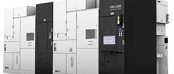
Canon has recently revealed its FPA-1200NZ2C, a nanoimprint semiconductor manufacturing tool that can be used to make advanced chips. The device uses nanoimprint lithography (NIL) technology as an alternative to photolithography, and can theoretically challenge extreme ultraviolet (EUV) and deep ultraviolet (DUV) lithography tools when it comes to resolution. Unlike traditional DUV and EUV photolithography equipment that transfers a circuit pattern onto a resist-coated wafer through projection, nanoimprint tool employs a different technique. It uses a mask, embossed with the circuit pattern, which directly presses against the resist on the wafer. This method eliminates the need for an optical mechanism in the pattern transfer process, which promises a more accurate reproduction of intricate circuit patterns from the mask to the wafer. In theory, NIL enables...
SK Hynix Starts Prepping for Next Semiconductor Boom with $11 Billion Memory Fab
When a major South Korean memory firm invests over $11 billion in a fab, that raises a couple of eyebrows. But when it comes within a major $100+ billion...
7 by Anton Shilov on 9/8/2022
TSMC and ASML: Demand for Chips Remains Strong, But Getting Fab Tools Is Hard
TSMC's revenue this year is going to set an all-time record for the company, thanks to high demand for chips as well as increased prices that its customers are...
13 by Anton Shilov on 7/21/2022
EUV Demand is Up: EUV Device Manufacturer ASML Beats Sales Estimates
Between the smartphone revolution, cloud computing, and the Internet of Things, the demand for cutting-edge chips has never been higher. And if you have any doubts about that, then...
46 by Anton Shilov on 10/16/2019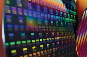
ASML, Carl Zeiss, and Nikon to Settle Legal Disputes Over Immersion Lithography
Embroiled for some time now in legal disputes concerning immersion lithography, ASML, Carl Zeiss, and Nikon, this week signed a memorandum of understanding relating to a plan to once...
10 by Anton Shilov on 1/25/2019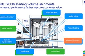
ASML Ships Twinscan NXT:2000i Scanner for 7nm and 5nm DUV
ASML, the company known for producing equipment for the manufacture of processors and semiconductors at foundries, has started to ship its new Twinscan NXT:2000i DUV (Deep Ultra Violet) scanner...
15 by Anton Shilov on 8/2/2018
The Future of Silicon: An Exclusive Interview with Dr. Gary Patton, CTO of GlobalFoundries
In our recent trip to GlobalFoundries Fab 8, its leading edge facility, we managed to spend some time with the C-level executive that controls the future of this part...
39 by Ian Cutress on 2/24/2018
Samsung’s 8LPP Process Technology Qualified, Ready for Production
Samsung this week announced that its 8LPP fabrication process, which it formally introduced earlier this year, had passed qualification tests. The manufacturing technology will be used to produce advanced...
35 by Anton Shilov on 10/19/2017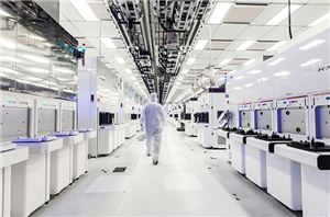
GlobalFoundries Details 7 nm Plans: Three Generations, 700 mm², HVM in 2018
Keeping an eye on the ever-evolving world of silicon lithography, GlobalFoundries has recently disclosed additional details about its 7 nm generation of process technologies. As announced last September, the...
76 by Anton Shilov on 6/23/2017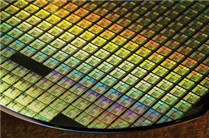
Samsung and TSMC Roadmaps: 8 and 6 nm Added, Looking at 22ULP and 12FFC
Samsung and TSMC have made several important announcements about the present and future of their semiconductor manufacturing technologies in March. Samsung revealed that it had shipped over 70 thousand...
89 by Anton Shilov on 5/5/2017


