Semiconductors
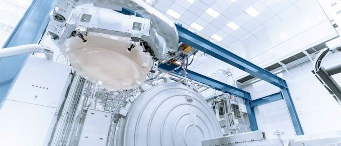
This week ASML is making two very important announcements related to their progress with high numerical aperature extreme ultraviolet lithography (High-NA EUV). First up, the company's High-NA EUV prototype system at its fab in Veldhoven, the Netherlands, has printed the first 10nm patterns, which is a major milestone for ASML and their next-gen tools. Second, the company has also revealed that it's second High-NA EUV system is now out the door as well, and has been shipped to an unnamed customer. "Our High-NA EUV system in Veldhoven printed the first-ever 10 nanometer dense lines," a statement by ASML reads. "Imaging was done after optics, sensors and stages completed coarse calibration. Next up: bringing the system to full performance. And achieving the same results in the...

Samsung's $15 Billion R&D Complex to Overcome Limits of Semiconductor Scaling
Samsung on Friday broke ground for a new semiconductor research and development complex which will design new fabrication processes for memory and logic, as well as conduct fundamental research...
26 by Anton Shilov on 8/19/2022
TSMC and ASML: Demand for Chips Remains Strong, But Getting Fab Tools Is Hard
TSMC's revenue this year is going to set an all-time record for the company, thanks to high demand for chips as well as increased prices that its customers are...
13 by Anton Shilov on 7/21/2022
Samsung Starts 3nm Production: The Gate-All-Around (GAAFET) Era Begins
Capping off a multi-year development process, Samsung’s foundry group sends word this morning that the company has officially kicked off production on its initial 3nm chip production line. Samsung’s...
22 by Ryan Smith on 6/30/2022
TSMC: N2 To Start With Just GAAFETs, Add Backside Power Delivery Later
When TSMC initially introduced its N2 (2 nm class) process technology earlier this month, the company outlined how the new node would be built on the back of two...
16 by Anton Shilov on 6/29/2022
TSMC to Customers: It's Time to Stop Using Older Nodes and Move to 28nm
We tend to discuss leading-edge nodes and the most advanced chips made using them, but there are thousands of chip designs developed years ago that are made using what...
20 by Anton Shilov on 6/29/2022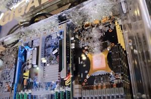
As HPC Chip Sizes Grow, So Does the Need For 1kW+ Chip Cooling
One trend in the high performance computing (HPC) space that is becoming increasingly clear is that power consumption per chip and per rack unit is not going to stop...
40 by Anton Shilov on 6/27/2022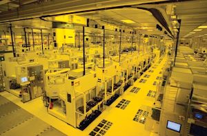
TSMC to Expand Capacity for Mature and Specialty Nodes by 50%
TSMC this afternoon has disclosed that it will expand its production capacity for mature and specialized nodes by about 50% by 2025. The plan includes building numerous new fabs...
13 by Anton Shilov on 6/16/2022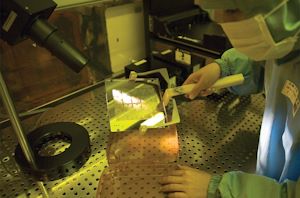
TSMC Unveils N2 Process Node: Nanosheet-based GAAFETs Bring Significant Benefits In 2025
At its 2022 Technology Symposium, TSMC formally unveiled its N2 (2 nm class) fabrication technology, which is slated to go into production some time in 2025 and will be...
24 by Anton Shilov on 6/16/2022
TSMC Readies Five 3nm Process Technologies, Adds FinFlex For Design Flexibility
Taiwan Semiconductor Manufacturing Co. on Thursday kicked off its 2022 TSMC Technology Symposium, where the company traditionally shares it process technology roadmaps as well as its future expansion plans...
44 by Anton Shilov on 6/16/2022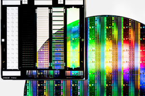
ASML High-NA Development Update: Coming to Fabs in 2024 - 2025
It took the semiconductor industry over a decade to prep everything needed for production of chips using extreme ultraviolet (EUV) lithography. It looks like it is going to take...
8 by Anton Shilov on 5/26/2022
Applied Materials Outlines Next-Gen Tools for 3nm and GAA Transistor Era
Last month Samsung Foundry quietly announced that it was set to begin producing chips using its 3GAE (3 nm-class, gate-all-around transistors, early) process technology in the second quarter. While...
17 by Anton Shilov on 5/12/2022
TSMC Roadmap Update: N3E in 2024, N2 in 2026, Major Changes Incoming
Taiwan Semiconductor Manufacturing Co. has solid plans for the next few years, but the foundry's manufacturing technology design cycles are getting longer. As a result, to address all of...
21 by Anton Shilov on 4/22/2022
AnandTech Interview with Dr. Ann Kelleher: EVP and GM of Intel’s Technology Development
It’s somewhat of an understatement to say that Intel’s future roadmap on its process node development is one of the most aggressive in the history of semiconductor design. The...
13 by Dr. Ian Cutress on 2/18/2022
A Visit to Intel’s D1X Fab: Next Generation EUV Process Nodes
On a recent trip to the US, I decided to spend some time criss-crossing the nation for a couple of industry events and spend some of the time visiting...
38 by Dr. Ian Cutress on 2/16/2022
Intel to Acquire Tower Semiconductor for $5.4B To Expand IFS Capabilities
Continuing their recent spending spree in expanding their foundry capabilities, Intel this morning has announced that it has struck a deal to acquire specialty foundry Tower Semiconductor for $5.4...
7 by Ryan Smith on 2/15/2022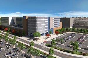
Intel Announces Ohio Fab Complex: 2 New Fabs For $20B, And Space For More
With fab expansions on tap across the entire semiconductor industry, Intel today is laying out their own plans for significantly increasing their production capacity by announcing their intention to...
114 by Ryan Smith on 1/21/2022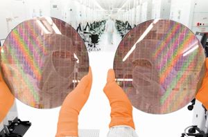
AMD and GlobalFoundries Wafer Supply Agreement Updated Once More: Now $2.1B Through 2025
In a short note published by AMD this afternoon as part of an 8-K filing with the US Securities and Exchange Commission, AMD is disclosing that the company has...
71 by Ryan Smith on 12/23/2021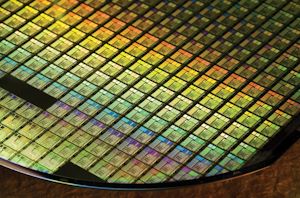
TSMC Unveils N4X Node: Extreme High-Performance at High Voltages
TSMC this week announced a new fabrication process that is tailored specifically for high-performance computing (HPC) products. N4X promises to combine transistor density and design rules of TSMC's N5-family...
42 by Anton Shilov on 12/17/2021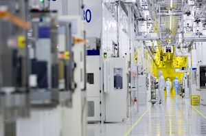
Semi CapEx to Hit $152 Billion in 2021 as Market on Track for $2 Trillion by 2035
Semiconductor makers have drastically increased their capital expenditures (CapEx) this year in response to unprecedented demand for chips that is going to last for years. Now the CEO of...
8 by Anton Shilov on 12/17/2021
Texas To Get Multiple New Fabs as Samsung and TI to Spend $47 Billion on New Facilities
After a year of searching for the right place of its new U.S. fab, Samsung this week announced that it would build a fab near Taylor, Texas. The company...
135 by Anton Shilov on 11/24/2021


