Samsung and TSMC Roadmaps: 8 and 6 nm Added, Looking at 22ULP and 12FFC
by Anton Shilov on May 5, 2017 9:30 AM ESTBeyond 10 nm at Samsung: 8 nm and 6 nm
Samsung’s 7 nm manufacturing technology is still expected to be the company’s first process to use extreme ultraviolet lithography (EUVL) for high-volume manufacturing (HVM) and that is going to happen sometimes in 2019 or later (risk production starts in the second half of 2018). In fact, the next several years down the road is where things will start to get interesting as Samsung announced another two new production technologies it has not talked about before: the 8 nm and the 6 nm processes.
| Industry FinFET Lithography Roadmap, HVM Start Data announced by companies during conference calls, press briefings and in press releases |
||||||||||||
| 2016 | 2017 | 2018 | 2019 | 2020 | 2021 | |||||||
| 1H | 2H | 1H | 2H | 1H | 2H | 1H | 2H | |||||
| GlobalFoundries | 14LPP | 7nm DUV | 7nm with EUV* | |||||||||
| Intel | 14 nm 14 nm+ |
14 nm++ 10 nm |
10 nm+ 10 nm++ |
|||||||||
| Samsung | 14LPP 14LPC |
10LPE | 10LPP | 8LPP 10LPU |
7LPP | 6 nm* (?) | ||||||
| SMIC | 28 nm** | 14 nm in development | ||||||||||
| TSMC | CLN16FF+ CLN16FFC | CLN10FF CLN16FFC |
CLN7FF CLN12FFC |
CLN12FFC/ CLN12ULP |
CLN7FF+ | 5 nm* (?) | ||||||
| UMC | 28 nm** | 14nm | no data | |||||||||
| *Exact timing not announced **Planar |
||||||||||||
Officially, Samsung says that both technologies will offer “greater scalability, performance and power advantages when compared to existing process nodes,” which obviously means that they are across the board better than Samsung’s current-gen 14 nm and 10 nm offerings. What is important is that Samsung also says that the “8 nm and the 6 nm will inherit all innovations from the latest 10 nm and the 7 nm technologies” respectively. This means that the 8 nm is set to keep using DUV and multi patterning (triple patterning or even quad patterning to be exact, but Samsung has not confirmed usage of the latter) for critical layers, whereas the 6 nm will come after 7 nm and will be Samsung’s second-generation EUV technology.
The only thing that Samsung confirms about its 8LPP manufacturing technology right now is the fact that this is a DUV-based process technology designed to shrink die size (i.e., increase transistor density) and frequency compared to the 10LPP fabrication process. Given the name of the technology and its key advertised advantages over direct predecessor, it is highly likely that the 8LPP will be used to make high-performance SoCs in 2019.
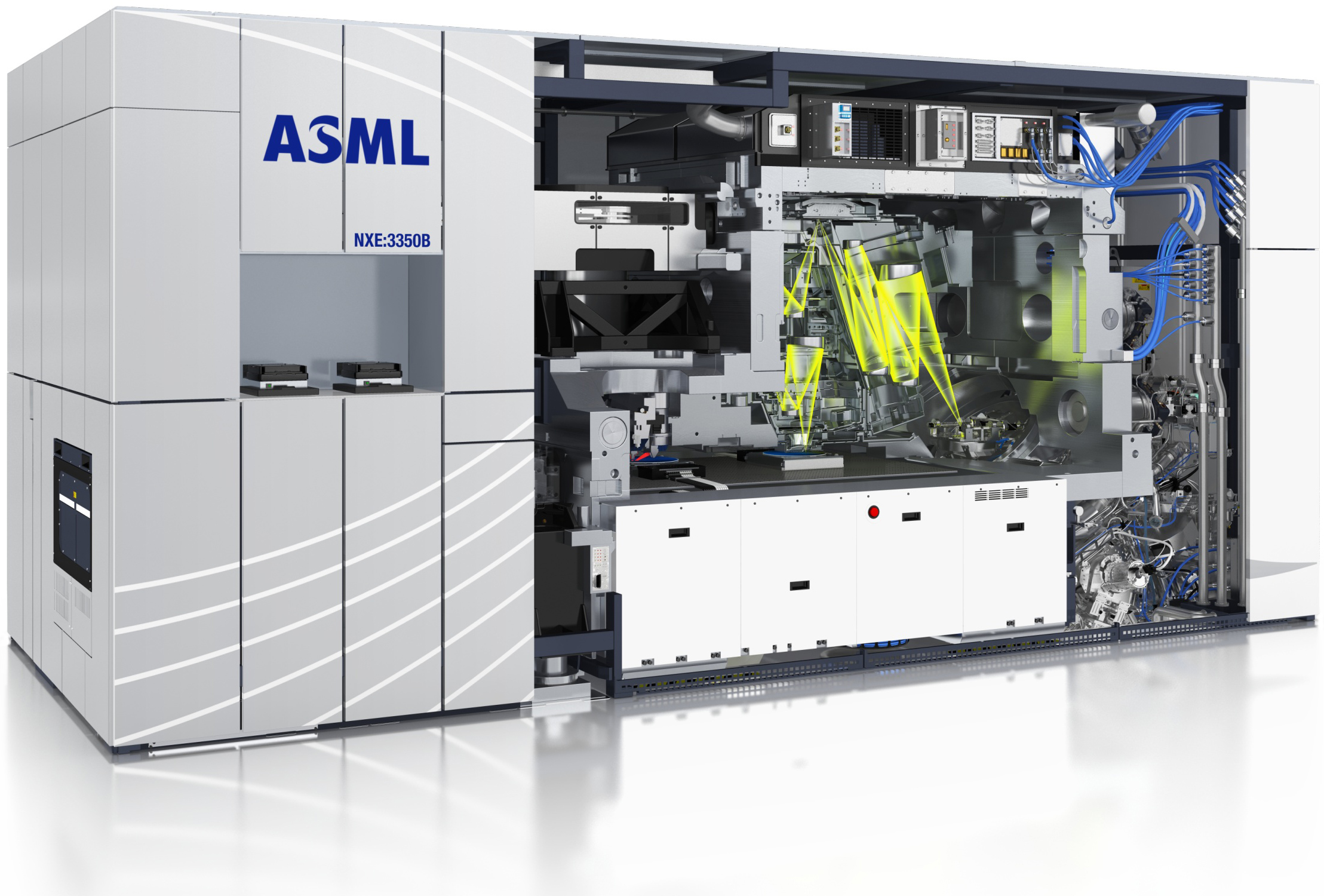
Since Samsung plans to start risk production using the 7LPP in the second half of 2018, the technology is hardly going to be used for high-volume manufacturing before the second half of 2019. Keeping in mind that Samsung now begins HVM using its leading-edge process technologies in October, it is possible that it is going to kick-off 7LPP HVM in fall 2019, but the 8LPP will be Samsung’s most advanced process technology for the better part of the year. Samsung does not mention timeframes for its 6 nm process technology and what to expect from it, but it is logical to assume that it will require more layers to be processed using ASML's EUV tools (like the NXE:3350B pictured above) in a bid to provide PPA advantages and it not be used for high-volume manufacturing before late 2020.
In March, Samsung only made brief announcements regarding its 10LPU, 8LPP and 6 nm process technology without disclosing their exact specifications or even PPA improvements targets. The addition of at least two more DUV technologies (the 10LPU and the 8LPP) in general may indicate that EUV may not be the best choice for all applications in 2019 – 2021, which is perfectly logical. Then again, we do not know how DUV and EUV technologies will co-exist early in the EUV era.
We are going to learn more about Samsung’s plans in the foundry industry in late May, when the company hosts its 2017 U.S Samsung Foundry Forum. So, we will have to wait for a couple of months for Samsung to disclose the whole picture regarding its upcoming process technologies.


89 Comments
View All Comments
Meteor2 - Sunday, May 7, 2017 - link
Do you mean Broadwell? But what's OC'd clock speed got to do with anything?jjj - Friday, May 5, 2017 - link
Pretty sure that the 10nm LPE perf claims are vs 14LPE not LPP as 27% higher perf is way too much.Anton Shilov - Friday, May 5, 2017 - link
Regarding the 10LPE vs 14LP*, I am not sure because we have two statements that contradict each other from Samsung.They stated the following in October:
"Samsung’s new 10nm FinFET process (10LPE) adopts an advanced 3D transistor structure with additional enhancements in both process technology and design enablement compared to its 14nm predecessor, allowing up to 30-percent increase in area efficiency with 27-percent higher performance or 40-percent lower power consumption."
http://www.anandtech.com/show/10765/samsung-10nm-m...
But if you look at the picture (from August) there (http://images.anandtech.com/doci/10765/dac.png), they mentioned ~30% performance increase at the same leakage power, which can considered as 27%... But if you happen to see some more up to date slides from Samsung, please let me know.
jjj - Saturday, May 6, 2017 - link
If they had anywhere close to 27% over 14LPP , they would have more design wins so it's safer to assume that "predecessor" means LPE. The phrasing itself is iffy, why "compared to ïts 14nm predecessor" and not just "compared to 14nm" - corporations are tricky like that.jjj - Sunday, May 7, 2017 - link
Hong Hao, senior vice president of the foundry business at Samsung Semiconductor "10nm brings a lot of benefits to our customers in terms of area scaling, performance and power or PPA. So overall, the PPA improvements are very substantial compared 14nm. We have compared that in terms of the performance, area and power to 14nm LPE. 14nm LPE is our first-generation finFET technology. We see up to a 30% area reduction with a 27% performance improvement or 40% lower power at the same performance."http://semiengineering.com/to-10nm-and-beyond/
willis936 - Friday, May 5, 2017 - link
Feynman is crying tears of joy in his grave. Intel is crying for another reason.melgross - Friday, May 5, 2017 - link
Oh, I don't know. It's acknowledged that Intel's current 14nm process is equivelant to other's 10nm processes, and likely their 10nm will be equivelant to other's 7nm.I don't think Intel has anything to,worry about for the next few years. I still doubt that 5nm will come about, at least, not as a real 5nm process, though it will likely be advertised as such.
But when that wall is reached, for everyone, then, long last, Intel will lose most of its process advantages. But that will be in 5 to 8 years, so there's still a long way to,go.
tarqsharq - Friday, May 5, 2017 - link
We'll have to see if we get another materials switch up off silicon.Some kind of graphene, maybe a photon based solution instead of electron?
Apparently quantum computing is only useful for certain types of operations, so that's not a magic bullet for speeding up all of our computing tasks.
Meteor2 - Friday, May 5, 2017 - link
I reckon we'll get real 5 nm, probably with quad patterning, possibly with a new transistor design, in around 2023-25. Difficult to see where we can go after that. Maybe that graphene stuff I suppose.vladx - Friday, May 5, 2017 - link
Nanotubes seems the most feasible solution.