AMD Unveils ‘Chiplet’ Design Approach: 7nm Zen 2 Cores Meet 14 nm I/O Die
by Anton Shilov on November 6, 2018 1:53 PM EST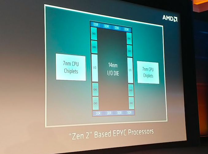
AMD on Tuesday disclosed some additional details about its upcoming codenamed Rome processor based on its Zen 2 microarchitecture. As it turns out, the company will use a new design approach with its next-generation EPYC CPUs that will involve CPU ‘chiplets’ made using TSMC’s 7 nm manufacturing technology as well as an I/O die made using a 14 nm fabrication process.
AMD’s chiplet design approach is an evolution of the company’s modular design it introduced with the original EPYC processors featuring its Zen microarchitecture. While the currently available processors use up to four Zen CPU modules, the upcoming EPYC chips will include multiple Zen 2 CPU modules (which AMD now calls ‘chiplets’) as well as an I/O die made using a mature 14 nm process technology. The I/O die will feature Infinity Fabrics to connect chiplets as well as eight DDR DRAM interfaces. Since the memory controller will now be located inside the I/O die, all CPU chiplets will have a more equal memory access latency than today’s CPU modules. Meanwhile, AMD does not list PCIe inside the I/O die, so each CPU chiplet will have its own PCIe lanes.
Separating CPU chiplets from the I/O die has its advantages because it enables AMD to make the CPU chiplets smaller as physical interfaces (such as DRAM and Infinity Fabric) do not scale that well with shrinks of process technology. Therefore, instead of making CPU chiplets bigger and more expensive to manufacture, AMD decided to incorporate DRAM and some other I/O into a separate chip. Besides lower costs, the added benefit that AMD is going to enjoy with its 7 nm chiplets is ability to easier bin new chips for needed clocks and power, which is something that is hard to estimate in case of servers.

This is a breaking news. We are updating the news story with more details.
Source: AMD


76 Comments
View All Comments
latentexistence - Tuesday, November 6, 2018 - link
IBM called, they want their Z196 mainframe multichip module with CPU dies around a storage controller die backFreckledTrout - Tuesday, November 6, 2018 - link
Imitation is the biggest form of flattery.hamiltenor - Tuesday, November 6, 2018 - link
If anyone reads this and wants more info, chapter 1.4.3 http://www.redbooks.ibm.com/abstracts/sg247833.htm...CheapSushi - Tuesday, November 6, 2018 - link
IBM helped AMD with their HT implementation on Zen. I bet they helped them with this MCM package too. What do you have against that? Why does it matter if it's similar? What's your agenda with this comment?nandnandnand - Wednesday, November 7, 2018 - link
"IBM helped AMD with their HT implementation on Zen."Do you have a source? I couldn't find this.
latentexistence - Wednesday, November 7, 2018 - link
I don’t have anything against that, I was making a joke because I think it’s cool.eastcoast_pete - Wednesday, November 7, 2018 - link
Nothing wrong with copying or imitating a successful design approach. Mainframe-on-a-chip is not a bad nickname to have.ravyne - Tuesday, November 6, 2018 - link
I'm not so sure PCIe is on the chiplets, I think it remains to be seen. There are advantages and disadvantages to either approach. Its a physical interface as well, so it scales poorly, but the pin-count is way lower than even a single DRAM controller.The chiplet/IO-die design opens lots of interesting questions though -- Is the L3 cache on the chiplet? If not, how much L2; if so, how much L3, and is there an L4 cache on the IO chiplet? Will the IO controller allow individual memory controllers to be partitioned into their own NUMA nodes? perhaps finer-grained bandwidth allocation via QoS mechanisms? Cloud providers / virtualization would love that.
Opportunities as well. Market-specific IO dies for Epic, Threadripper, and Ryzen? What about APUs? I could see the GPU compute/control/cache being located on a 7nm chiplet of its own, with a 14/12nm IO chiplet having the display interfaces and framebuffer (maybe an EDRAM large enough for multiple render targets, perhaps configured as a general victim cache as intel's EDRAM is, or maybe with a single HBM2 interface).
ravyne - Tuesday, November 6, 2018 - link
I do also wonder if manufacturing the IO die at 14nm helps them keep their contractual commitments with GloFo, now that they're not moving their production lines to 7nm. Looking at the size of the IO die, it looks roughly equal in size to 3-4 Zen1 dies in 14nm.DigitalFreak - Tuesday, November 6, 2018 - link
It would be interesting if they put PCI-E on the I/O chip and had an extremely high bandwidth interconnect to each chiplet. I'd love to see an 8 core Ryzen 3xxx with 40+ PCI-E lanes.