The Intel 12th Gen Core i9-12900K Review: Hybrid Performance Brings Hybrid Complexity
by Dr. Ian Cutress & Andrei Frumusanu on November 4, 2021 9:00 AM ESTPower: P-Core vs E-Core, Win10 vs Win11
For Alder Lake, Intel brings two new things into the mix when we start talking about power.
First is what we’ve already talked about, the new P-core and E-core, each with different levels of performance per watt and targeted at different sorts of workloads. While the P-cores are expected to mimic previous generations of Intel processors, the E-cores should offer an interesting look into how low power operation might work on these systems and in future mobile systems.
The second element is how Intel is describing power. Rather than simply quote a ‘TDP’, or Thermal Design Power, Intel has decided (with much rejoicing) to start putting two numbers next to each processor, one for the base processor power and one for maximum turbo processor power, which we’ll call Base and Turbo. The idea is that the Base power mimics the TDP value we had before – it’s the power at which the all-core base frequency is guaranteed to. The Turbo power indicates the highest power level that should be observed in normal power virus (usually defined as something causing 90-95% of the CPU to continually switch) situation. There is usually a weighted time factor that limits how long a processor can remain in its Turbo state for slowly reeling back, but for the K processors Intel has made that time factor effectively infinite – with the right cooling, these processors should be able to use their Turbo power all day, all week, and all year.
So with that in mind, let’s start simply looking at the individual P-cores and E-cores.
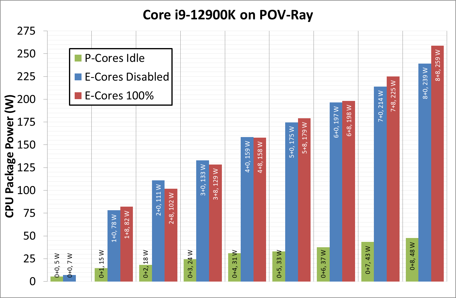
Listed in red, in this test, all 8P+8E cores fully loaded (on DDR5), we get a CPU package power of 259 W. The progression from idle to load is steady, although there is a big jump from idle to single core. When one core is loaded, we go from 7 W to 78 W, which is a big 71 W jump. Because this is package power (the output for core power had some issues), this does include firing up the ring, the L3 cache, and the DRAM controller, but even if that makes 20% of the difference, we’re still looking at ~55-60 W enabled for a single core. By comparison, for our single thread SPEC power testing on Linux, we see a more modest 25-30W per core, which we put down to POV-Ray’s instruction density.
By contrast, in green, the E-cores only jump from 5 W to 15 W when a single core is active, and that is the same number as we see on SPEC power testing. Using all the E-cores, at 3.9 GHz, brings the package power up to 48 W total.
It is worth noting that there are differences between the blue bars (P-cores only) and the red bars (all cores, with E-cores loaded all the time), and that sometimes the blue bar consumes more power than the red bar. Our blue bar tests were done with E-cores disabled in the BIOS, which means that there might be more leeway in balancing a workload across a smaller number of cores, allowing for higher power. However as everything ramps up, the advantage swings the other way it seems. It’s a bit odd to see this behavior.
Moving on to individual testing, and here’s a look at a power trace of POV-Ray in Windows 11:
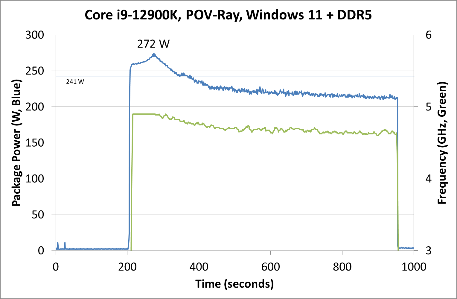
Here we’re seeing a higher spike in power, up to 272 W now, with the system at 4.9 GHz all-core. Interestingly enough, we see a decrease of power through the 241 W Turbo Power limit, and it settles around 225 W, with the reported frequency actually dropping to between 4.7-4.8 GHz instead. Technically this all-core is meant to take into account some of the E-cores, so this might be a case of the workload distributing itself and finding the best performance/power point when it comes to instruction mix, cache mix, and IO requirements. However, it takes a good 3-5 minutes to get there, if that’s the case.
Intrigued by this, I looked at how some of our other tests did between different operating systems. Enter Agisoft:
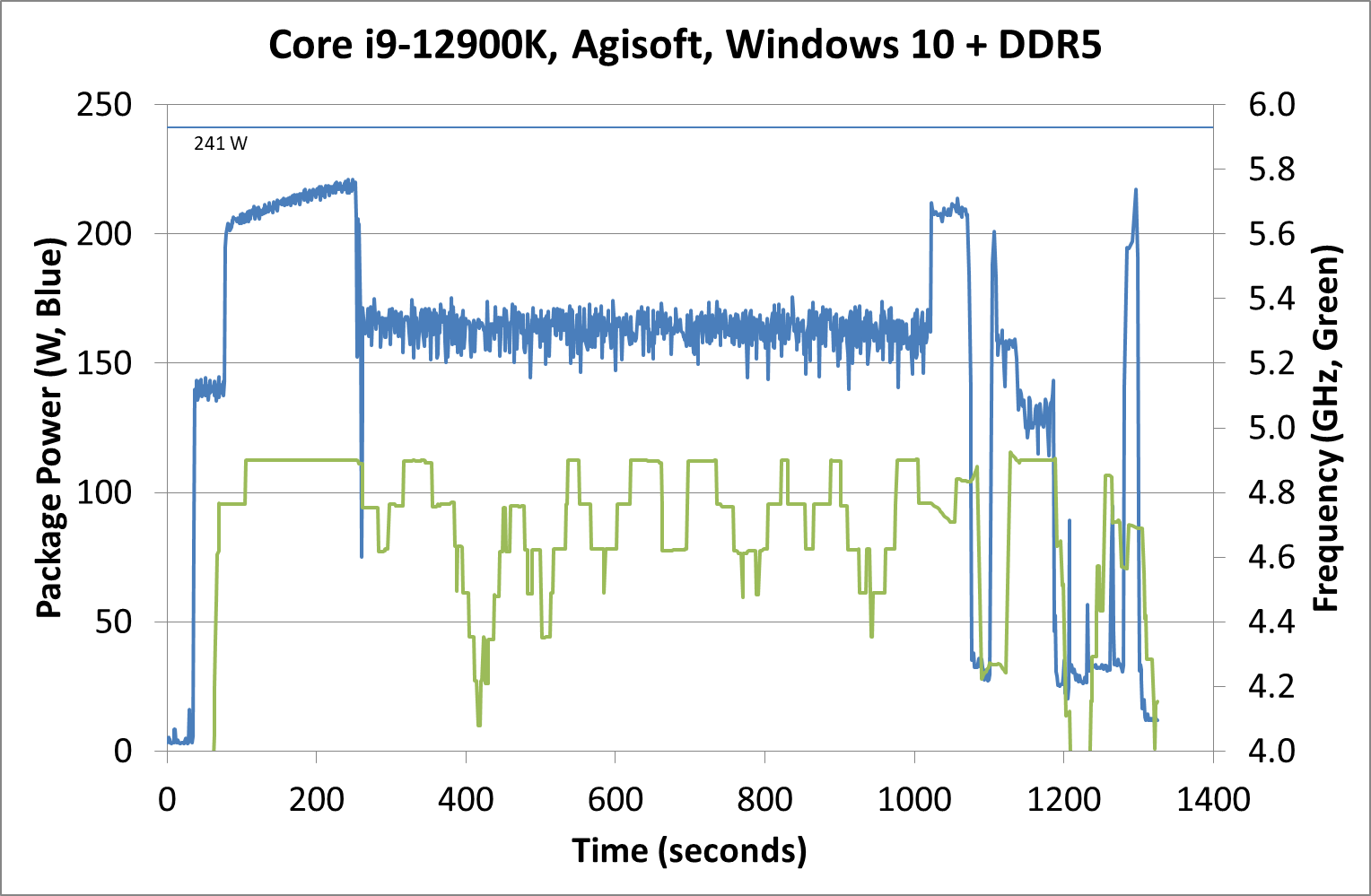
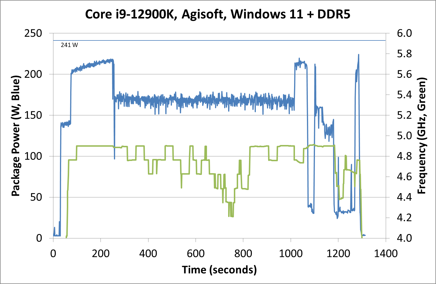
Between Windows 10 and Windows 11, the traces look near identical. The actual run time was 5 seconds faster on Windows 11 out of 20 minutes, so 0.4% faster, which we would consider run-to-run variation. The peaks and spikes look barely higher in Windows 11, and the frequency trace in Windows 11 looks a little more consistent, but overall they’re practically the same.
For our usual power graphs, we get something like this, and we’ll also add in the AVX-512 numbers from that page:
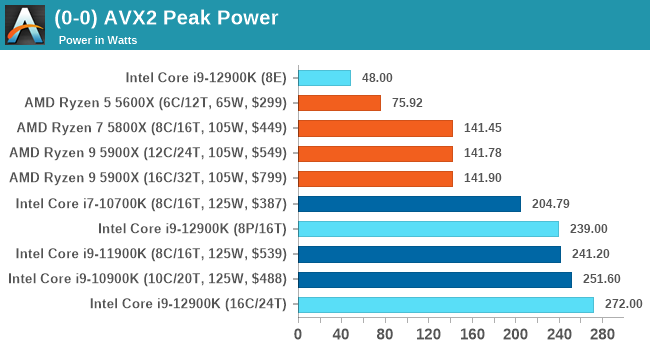
Compared to Intel’s previous 11th Generation Processor, the Alder Lake Core i9 uses more power during AVX2, but is actually lower in AVX-512. The difficulty of presenting this graph in the future is based on those E-cores; they're more efficient, and as you’ll see in the results later. Even on AVX-512, Alder Lake pulls out a performance lead using 50 W fewer than 11th Gen.
When we compare it to AMD however, with that 142 W PPT limit that AMD has, Intel is often trailing at a 20-70 W deficit when we’re looking at full load efficiency. That being said, Intel is likely going to argue that in mixed workloads, such as two software programs running where something is on the E-cores, it wants to be the more efficient design.


474 Comments
View All Comments
mode_13h - Sunday, November 7, 2021 - link
I'm not even going to say this is a bad idea. The problem is that it's a big change and Intel normally prepares the software developer community for big new ISA extensions a year+ in advance!Again, what you're talking about is an ABI change, which is a big deal. Not only that, but to require code to handle dynamically switching between AVX2 and AVX-512 paths means that it can't use different datastructures for each codepath. It even breaks the task pre-emption model, since there need to be some limitations on where the code needs to have all its 512-bit registers flushed so it can handle switching to the AVX2 codepath (or vice versa).
This adds a lot of complexity to the software, and places a greater testing burden on software developers. All for (so far) one CPU. It just seems a bit much, and I'm sure a lot of software companies would just decide not to touch AVX-512 until things settle down.
GeoffreyA - Sunday, November 7, 2021 - link
My view on this topic is that Intel made a sound decision disabling AVX512. Some of the comments are framing it as if they made a mistake, because the tech community discovered it was still there, but I don't see any problem. Only, the wording was at fault, this controversial "fused off" statement. And actually, the board makers are at fault, too, enabling a hidden feature and causing more confusion.On the question of whether it's desirable, allowing one core with the instructions and another without, would've been a recipe for disaster---and that, too, for heaven knows what gain. The simplest approach was bringing both cores onto the same footing. Indeed, I think this whole P/E paradigm is worthless, adding complexity for minimal gain.
Oxford Guy - Monday, November 8, 2021 - link
‘Intel made a sound decision disabling AVX512’That’s not what happened.
O-o-o-O - Sunday, November 7, 2021 - link
Really? Our tech guys tried out Xeon Phi but couldn't make use of it. Years later, Xeon Phi was abruptly discontinued due to lack of demand. GPGPUs are much easier to handle.Yeah, coding cost and risks aside, it's interesting to see complex work of art in the modern CPU. But I'd rather wish for expansion of GPU support (like shared memory and higher band-width).
kwohlt - Sunday, November 7, 2021 - link
My understanding is that Raptor Lake's change is replacing Golden Cover P cores with Raptor Cove P cores, doubling Gracemont E-Cores per SKU, and using the same Intel 7 process. Granted, it's all leaks at this point, but with Gracemont being reused for Raptor Lake, I don't expect AVX-512 next year either.mode_13h - Monday, November 8, 2021 - link
> Raptor Lake's change is ... doubling Gracemont E-Cores ... using the same Intel 7 process.I was merely speculating that this *might* just be a transient problem. If they're using the same process node for Raptor Lake, which seems very plausible, then it's understandable if they don't want to increase the size or complexity of their E-cores.
However, there's some precedent, in the form of Knights Landing, where Intel bolted on dual AVX-512 pipelines + SMT4 to a Silvermont Atom core. And with a more mature Intel 7 node, perhaps the yield will support the additional area needed for just a single pipe + 512-bit registers. And let's not forget how Intel increased the width of Goldmont, yet simply referred to it as Goldmont+.
So, maybe Raptor Lake will use Gracemont+ cores that are augmented with AVX-512. We can hope.
GURU7OF9 - Saturday, November 6, 2021 - link
The is by far the best review I have read so far.A great comparison I would love to see just out of curiouslty would be to see P core only benchmarks and then e core only benchmarks! We could gain a much better understanding of the capabilities and performance of both .
This would bring a little bit of familiarity back to benchmarking .
nunya112 - Saturday, November 6, 2021 - link
the only info provided was its on intels new process 7 node. what does that mean? are they using TSMC and at 7nm? or did they finally crack 7nm at Intel?mode_13h - Sunday, November 7, 2021 - link
"Intel 7" is the process node formerly known as "10 nm ESF" (Enhanced SuperFin), which is the 4th generation 10 nm process, counting by the revisions they've introduced between the different products based on it. They like to pretend that Cannon Lake didn't happen, but that's why Ice Lake was actually 10 nm+ (2nd gen).They rebranded 10 nm ESF as "Intel 7" for marketing reasons, as explained here:
https://www.anandtech.com/show/16823/intel-acceler...
Hossein - Sunday, November 7, 2021 - link
It's funny that most reviewers are conveniently silent about the fact that there are quite a 'few' games which are incompatible AL.