Adesto EcoXiP: Optimizing Memory Interfaces For Embedded Systems
by Billy Tallis on November 17, 2016 11:00 AM ESTThere is no Moore's Law for flash memory. Unlike transistors, flash memory cells can no longer be made any smaller or faster without incurring reliability tradeoffs that negate the benefits of a process shrink. This has forced the solid state storage industry to look elsewhere for potential improvements. The long-term hopes are focused on a variety of non-volatile memory technologies that are years away from reaching the cost and density of NAND flash, but promise vast improvements to endurance, latency or power consumption. In the meantime, the challenge is to reduce cost or increase the performance that is possible from flash memory by changing how it is organized and accessed.
In the PC SSD market, two major shifts are underway to satisfy the need for continued progress in spite of the stagnation of the fundamental underlying memory cell technology. 3D NAND flash is replacing planar NAND flash, enabling density to continue growing and cost per bit to decline further while keeping the memory cell large enough to provide acceptable write endurance. Further up the storage stack, PCIe and the NVMe protocol allow for substantial improvements in throughput and latency as compared with the SATA interface.
But the SSD market is hardly the only outlet for flash memory technology. 3D NAND flash is beginning to replace planar NAND in smartphones and memory cards, and faster host interfaces are available for those markets. For even smaller embedded systems, NOR flash is still used. In these markets, low power and cost are often a higher priority than capacity and performance. The increasing popularity of the Internet of Things means many of those devices now have to include full network stacks supporting IPv6 and LTE, and thus their storage requirements have increased substantially.
Adesto is one of the many companies developing a new non-volatile memory, but their conductive bridging RRAM (CBRAM) so far only offers sub-megabit capacities. Adesto's flash memory products are tailored for low-power embedded and IoT applications. Optimizing a memory product for these uses typically means using a low pin count interface like SPI and implementing extremely low-power sleep states. Erase block sizes are tuned to suit expected access patterns.
Adesto's latest family of flash memory products makes some more drastic changes. Their EcoXiP line is intended for systems with an Execute In Place (XiP) memory architecture where the processor fetches code directly from flash into the instruction cache rather than loading it into a separate DRAM or SRAM bank. XiP systems save money by requiring less RAM, but at the cost of making CPU performance highly dependent on the performance of the flash.
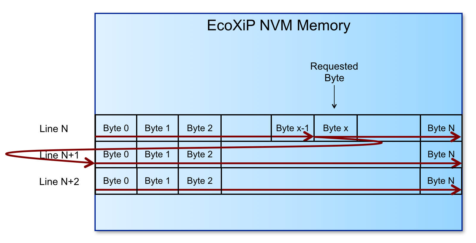
EcoXiP introduces a new mode for reading data that is designed to minimize the latency and command overhead of handling instruction cache misses. When the processor needs to branch to an address that is not in the instruction cache, it can issue a read request starting at the exact byte that is required. After the unavoidable latency of issuing the command and waiting for the flash to be read, the EcoXiP memory begins streaming the data from the requested byte. After reaching the end of the cache line the EcoXiP memory automatically wraps around to the earlier portion of the cache line so that the processor can fully populate that cache line while execution continues. The EcoXiP memory can then optionally proceed to sequentially stream subsequent cache lines in-order without requiring new read commands and addresses to be issued. Adesto estimates that the combination of delivering the most important byte first and enabling fast pre-fetching can increase effective CPU performance by over 40% for the case of a 266MHz processor using a 133MHz Octal SPI interface to flash with 100ns access time.
EcoXiP memory devices also support configuring the memory to behave as two independent banks. A single NOR flash bank cannot perform reads and writes simultaneously, which for an XiP device typically means the flash has to be treated as effectively a ROM device. Partitioning the device into separate banks allows the same chip to be used for both XiP operation and data logging, or to allow a software update to be installed to the second bank without suspending execution from the first bank.
The obvious downside to these innovations is that it is non-standard behavior. SPI itself is not a formal standard, but it is a widely supported de facto standard that has been around for decades, and JEDEC has defined a standard for querying the capabilities of SPI flash devices (similar to SPD and XMP for DRAM modules). Adesto's protocol extensions require modifications to the processor's memory controller and using EcoXiP will influence other system-level design decisions about memory and storage. Adesto has secured the support of microcontroller vendor NXP and IP vendors Synopsys and Mobiveil, so they should have no trouble building the market of devices that support EcoXiP memory.
Just as NVMe's benefits over SATA will continue to help as SSDs using new persistent memories like 3D XPoint instead of flash come to market, Adesto's protocol optimizations are not limited to just flash memory devices. Since most new persistent memory technologies will initially be available in capacities too small to directly replace NAND flash for SSD use and many of those technologies will be more economical to use as discrete memory devices rather than embedded memory integrated on SoCs, we will probably see several vendors producing specialized memory devices with optimizations similar to those used in Adesto's EcoXiP.
EcoXiP memory is initially available as a 32Mb (4MB) device rated for 100,000 Program/Erase cycles and 20 year data retention, with a maximum transfer rate of 266MB/s. Capacities up to 128Mb (16MB) are planned.
Source: Adesto


7 Comments
View All Comments
ddriver - Thursday, November 17, 2016 - link
"Unlike transistors, flash memory cells can no longer be made any smaller or faster without incurring reliability tradeoffs that negate the benefits of a process shrink."It would be a real shocker to learn that flash memory is made of ... transistors...
And while it is true that flash memory becomes progressively unreliable as process shrinks, the same hindrance is intrinsic to all other circuitry as well. Maybe not as pronounced in detriment but apparent nonetheless.
patrickjchase - Thursday, November 17, 2016 - link
What you describe is critical-word-first cache line fill. It's been around for ages. Nothing to see here.Also, I've worked on several embedded products that executed in place from flash. Nothing new there, either.
evancox10 - Sunday, November 20, 2016 - link
Have also worked on embedded microcontroller products and agree with you. This article comes off as a puff piece/PR regurgitation.However, I'm not sure I've seen this exact type of addressing mode in current QSPI flashes. Normally you are either in linear or wraparound mode. This, on the other hand, performs a single wraparound and then proceeds with linear access for the next lines.
This single, marginal improvement is really not all that amazing.
Daniel Egger - Thursday, November 17, 2016 - link
> There is no Moore's Law for flash memory.Nonsense. Of course Moore's law also applies to flash memory: The "law" is simply the observation that the complexity of circuits doubles about every two years; it's actually even easier to determine for flash because one simply needs to look at the available SSD sizes over time...
BrokenCrayons - Thursday, November 17, 2016 - link
First off, I think the fact that an observation about integrated circuits made by Moore has been taken way too far over the intervening years to the point where it's widely misunderstood, taken far out of its original context, and doesn't say anything meaningful when invoked by people to support a discussion. I really would be a bit happier if we put it behind us in the same tech graveyard where the Bill Gates 640KB of RAM myth and the dollar sign-substituted Micro$oft also ought to be buried.However, since we're already invoking...Moore's comment wasn't about complexity doubling, but about the number of transistors in an IC. Of course, with increased transistor counts there's an implied increase in complexity, but there are lots of ways to add transistors to an integrated circuit that won't make the design inherently more complex.
Daniel Egger - Thursday, November 17, 2016 - link
Thanks for rephrasing my point in your own words.BrokenCrayons - Friday, November 18, 2016 - link
Eek, I'm sorry! That sounds kind of like sarcasm and I don't want you to feel upset. I was really just ranting about Moore's Law in general and not specifically about your misunderstanding. Please don't interpret my comment as something worth getting triggered about. I was just trying to clear up confusion.