Intel Lists Knights Mill Xeon Phi on ARK: Up to 72 cores at 320W with QFMA and VNNI
by Ian Cutress on December 19, 2017 7:00 AM EST- Posted in
- Enterprise
- Intel
- MIC
- Xeon Phi
- Knights Mill
- AVX-512
- AVX512
- KNM
Today it was noticed, without any fanfare from Intel, that Knights Mill information has been uploaded to Intel’s specification database ARK. There are three known SKUs so far, with up to 72 cores and a 320W TDP. The Xeon Phi 'Knights Mill' products are a new iteration on the older 'Knights Landing' family, with a silicon change for additional AVX-512 instructions. As far as we can tell, these parts will only be available as socketable hosts and not as PCIe add-in cards.
In Intel’s approach to AI and compute and the data center, according to their talk at Hot Chips earlier this year, has multiple solutions depending on the workload. The Xeon Scalable Platform is meant for the widest variety of workloads, Xeon Phi for parallel acceleration and AI training, FPGAs for deep learning inference efficiency and the Crest family with dedicated deep learning by design. Each segment has its own roadmap, and the Xeon Phi roadmap has been somewhat confusing of late.
Moving from the 45nm Knights Ferry in 2010, Intel released 22nm Knights Corner in 2012 and 14nm Knights Landing in 2016. Last year, Intel had a contract with the Argonne National Laboratory to build the Aurora supercomputer at using 10nm Knights Hill (KNH) by 2020, which was the original successor to Knights Landing, however the KNH project was officially scrapped last month (Nov 2017) for various reasons, some citing Intel’s delay in releasing 10nm silicon. Intel still intends to follow through with the Aurora contract by 2021, it should be noted.
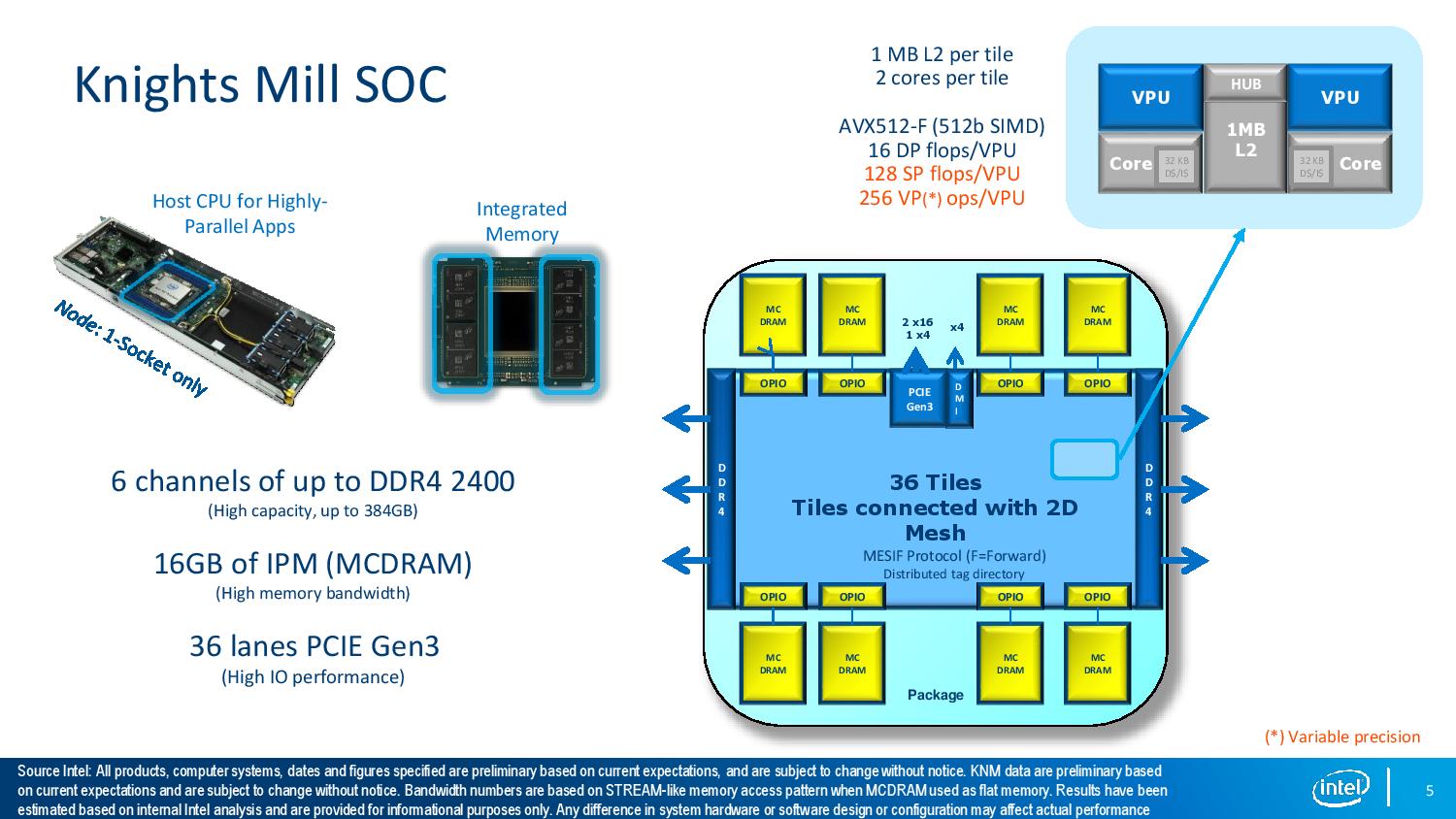
The new successor to Knights Landing (KNL) is Knights Mill (KNM), which was detailed back at Hot Chips. For the most part, the KNL and KNM chips are almost identical in core counts, frequencies, 36 PCIe 3.0 lanes, using 16GB of high-bandwidth MCDRAM and having six DRAM channels, but KNM offers a small design tweak to allow for better utilization of its AVX-512 units through supporting new sets of AVX-512 instructions as well as a small amount of silicon redesign. For pure performance metrics, this change means that Knights Mill offers only half of the double-precision performance of Knights Landing, but up to 2x in single precision and 4x with variable precision.
| Intel Xeon Phi x205 Family (Knights Mill) | |||||||
| Cores | Base | Turbo | L2 | TDP | DRAM | TCASE | |
| 7295 | 72 / 288 | 1.50 GHz | 1.60 GHz | 36 MB | 320W | DDR4-2400 | 77ºC |
| 7285 | 68 / 272 | 1.30 GHz | 1.40 GHz | 34 MB | 250W | DDR4-2400 | 72ºC |
| 7235 | 64 / 256 | 1.30 GHz | 1.40 GHz | 32 MB | 250W | DDR4-2133 | 72ºC |
The three parts are officially members of the Xeon Phi x205 family, and match their x200 family members where the product numbers align (eg 7290 and 7295). The 7295 has the most cores and threads, with a higher frequency, more total L2 cache, support for DDR4-2400 and the higher temperature support. The 7285 is the middle of the pack, while the low end 7235 gives up some memory support, with only up to DDR4-2133.
The previous generation parts had some integrated OmniPath fabric versions (such as the 7290F) which do not seem to have migrated over to Knights Mill yet, though could potentially in the future. Each of the parts are similar to KNL, using 36 tiles of two cores, all connected with the 2D mesh, and each tile sharing 1MB of L2 cache with one VPU per core.
On the specification side, everything seems pretty much by the book for core counts and frequencies. The one number that stands out is the 320W for the Xeon Phi 7295. This is a high power consumption number for a socketed processor, and if my memory serves me correctly, this is the highest TDP ever assigned to an Intel socketed CPU. This isn't the highest for a socketed processor though - IBM quoted 300-350W for its z14 hardware earlier this year, although it can go up to 500W on consumer request. The reason for this dramatic increase in Intel’s TDP number (we suspect) is three-fold: one, to catch more processors off the production line into the relevant voltage/frequency window, and two, the new instructions offer better utilization of the silicon, and three: double-pumped execution.
| AVX-512 Support Propogation by Various Intel CPUs | ||||||
| Xeon, Core X | General | Xeon Phi | ||||
| Skylake-SP | AVX512BW AVX512DQ AVX512VL |
AVX512F AVX512CD |
AVX512ER AVX512PF |
Knights Landing | ||
| Cannon Lake | AVX512VBMI AVX512IFMA |
AVX512_4FMAPS AVX512_4VNNIW |
Knights Mill | |||
| Ice Lake | AVX512_VNNI AVX512_VBMI2 AVX512_BITALG AVX512+VAES AVX512+GFNI AVX512+VPCLMULQDQ |
AVX512_VPOPCNTDQ | ||||
| Source: Intel Architecture Instruction Set Extensions and Future Features Programming Reference (pages 12 and 13) | ||||||
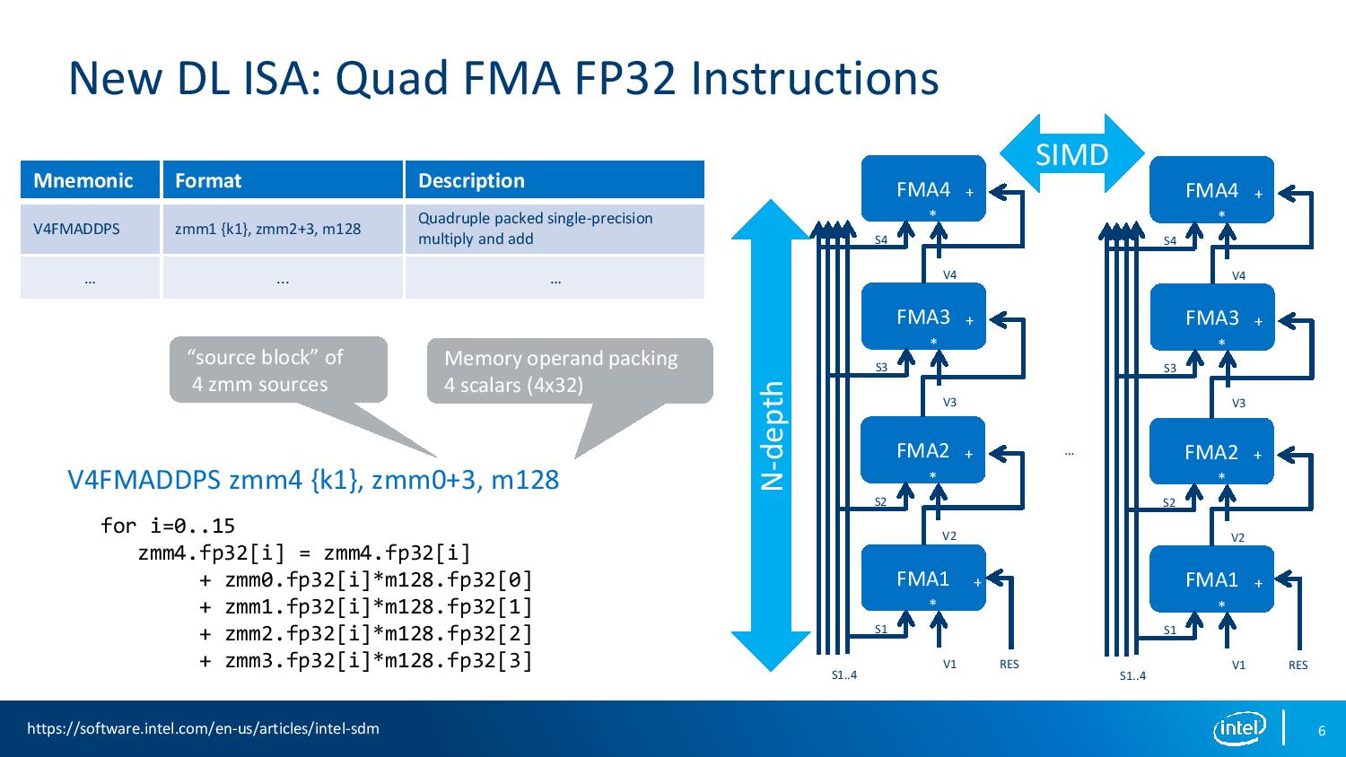
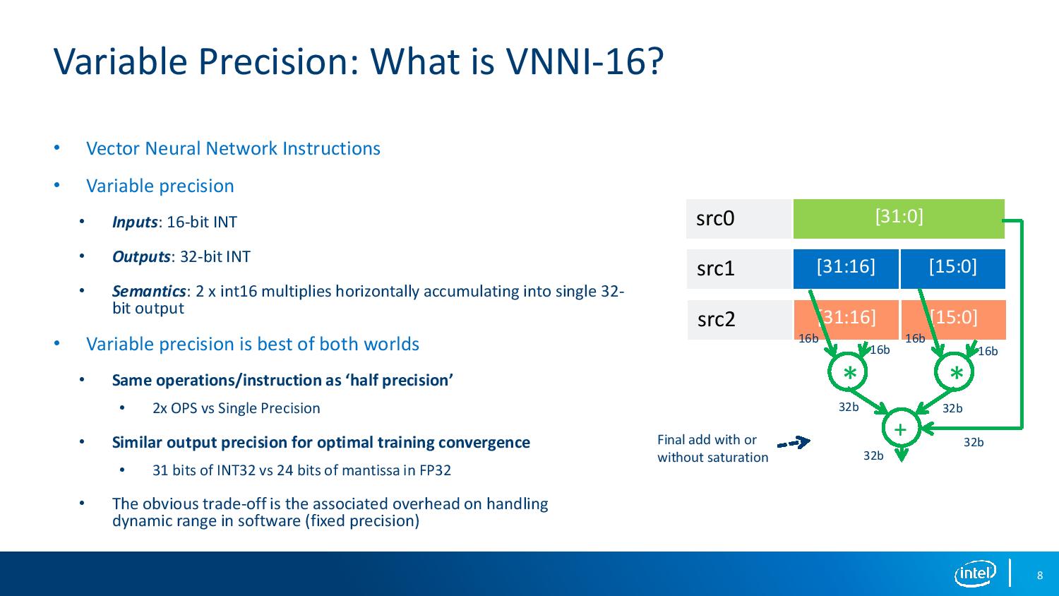
The two headline changes on instructions for the new parts revolve around support for Quad FMA (QFMA, or 4FMAPS) for 32-bit floating point, and Vector Neural Network Instructions (VNNI) for 16-bit integers. To do this required changing the execution ports on the core.
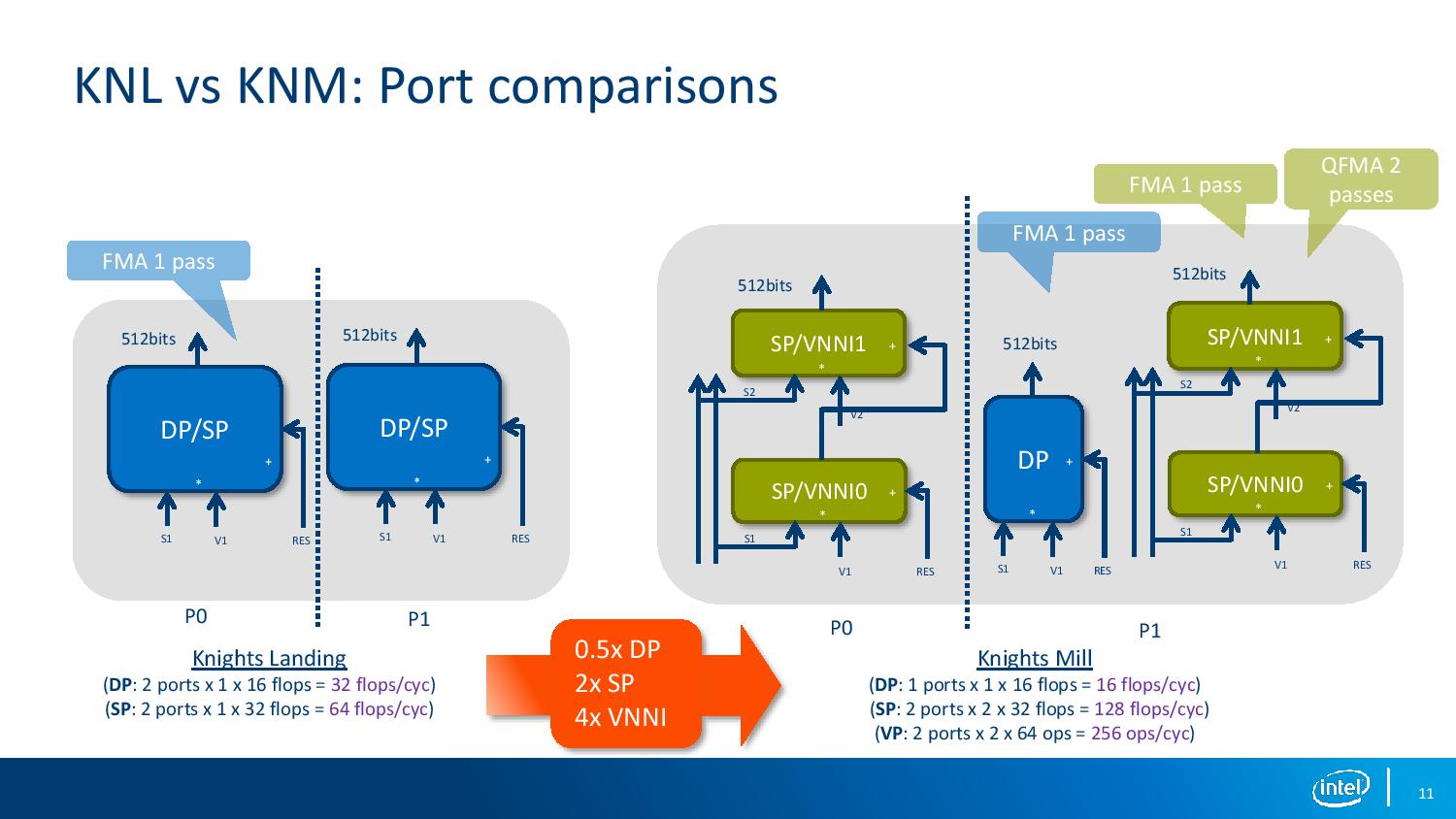
Previously each VPU per core would offer identical 512-bit interfaces to the AVX-512 unit, supporting single precision (SP) and double precision (DP) math, with any half-precision (HP) falling under an SP block. In the new design, the ports are asymmetrical: the SP/DP block is split into a separate DP and SP/VNNI blocks, with one DP block removed (likely due to the size of the SP/VNNI block). This is best shown in the diagram above, though it means that DP performance is halved (2 blocks to 1), but SP performance is doubled (2 blocks to 4) and VNNI performance is quadrupled (2 SP blocks to 4 HP blocks).
The QFMA implementation allows for sequential fused-multiply-add to accumulate over four sets of calculations with a single instruction. Technically this adds latency, so the calculation needs enough ILP to hide the latency, but offers a single target for the vector accumulator and allows packing together of 12 aligned cycles in DRAM. Each FMA takes about 3 cycles.
For VNNI, the core takes two 16-bit integer inputs to give one 32-bit integer output for a horizontal dot product operation. The reason for using integer math here is two-fold: one, it enables 31-bits of INT prevision vs 24-bits of mantissa in FP, but also because IEEE standards are easier to implement in INT math.
Support for these new instructions and the silicon redesign means two things: one, the decoder potentially can work less, with more math being packed into a single instruction, but also caters to what Intel thought was a bottleneck in AVX-512 utilization: not enough codes were using all the AVX-512 unit all the time. This is designed to help increase utilization, and therefore would increase power consumption.
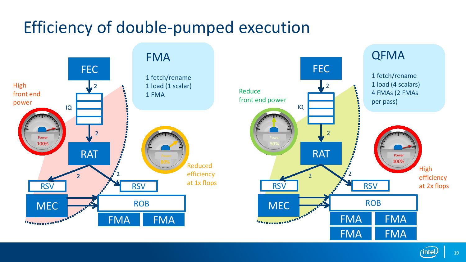
The other part of the equation is double pumping the AVX-512 unit, ensuring that the unit is fed at all times while reducing decode power.
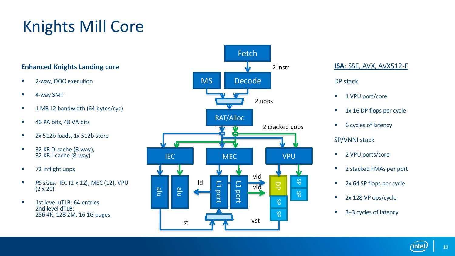
Overall the KNM core is looks almost identical to the KNL core, aside from the VPU port changes. It still decodes 2-ops per cycle but gives out-of-order execution with 72-inflight micro-ops. To hide a lot of the latency, 4-way hyperthreading is enabled, hence why a 64-core part gives 256 threads.
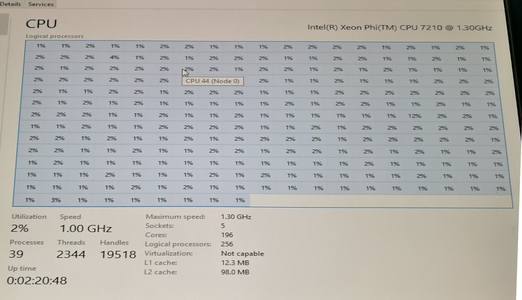
Our KNL 7210 Sample
Intel’s major partners already have Knights Mill available for customers, although list pricing is currently not in Intel's Price List. It’s interesting that the data being added to Intel’s ARK platform wasn’t accompanied by any announcement, and seems to be a low-key affair.
Source: Wikichip on Twitter, Intel ARK
Additional
Something we missed in our first look at the specifications. Over the older Knights Landing parts, the new Knights Mill parts also support Intel virtualization technologies, specifically VT-d, VT-x and EPT.


75 Comments
View All Comments
Elstar - Tuesday, December 19, 2017 - link
Having worked with Knights Landing, I can say that it is a weird "Xeon". When its fast, its very fast. But in general, it's an unforgiving CPU due to the shallow OOO pipeline, lack of shared LLC, and an instruction decoder that struggles to keep up.Elstar - Tuesday, December 19, 2017 - link
Also, the high-bandwidth MCDRAM and 4-way SMT can be unforgiving too. The former because it has worse latency than normal memory, and the latter because the pipeline frontend is statically partitioned.ddrіver - Tuesday, December 19, 2017 - link
If you use it for the right job that shouldn't be a problem.mode_13h - Tuesday, December 19, 2017 - link
I'm actually going to agree. @Elstart is missing the point - SMT and low clockspeeds make the *apparent* latency of MCDRAM much lower.I don't know if it's true that the absolute latency of MCDRAM is higher, but one benefit of SMT is to hide memory latency. If your workload has enough concurrency, then it works just fine.
Elstar - Tuesday, December 19, 2017 - link
I'm talking about programming in practice, not theory. MCDRAM latency on Knights Landing in practice is about 150 ns, whereas normal DRAM is about 128 ns. And yes, in theory, a great SMT implementation makes it easy to hide latency, but the SMT implementation on Knights Landing is quite basic. For example, if you average 3 busy threads on each CPU over the course of your app, then the statically partitioned frontend means that you get 3/4 of the available (and already feeble) decoder bandwidth.This all being said, I think Xeon Phi is a great CPU. It just isn't a forgiving like a normal Xeon. That is my only point here.
rbanffy - Wednesday, December 20, 2017 - link
Is each core still running fixed time slots like the original Phi? I though that feature was gone.mode_13h - Wednesday, December 20, 2017 - link
The issue might be your perspective. You're saying these cores aren't as well-optimized as a normal server core, but that's actually by design. The philosophy behind this chip is similar to that of GPUs - make the cores really simple and energy-efficient, then pack a ton of them on a single die. Sure, you could improve pipeline utilization, but would it yield a net improvement in power-efficiency? How many fewer cores would fit on a die? Would you then have to boost the memory clock to keep all the cores fed? You're really not looking at this as a tradeoff.So, while I'm not very familiar with KNM's SMT implementation, it doesn't surprise me that it stalls in places their bigger cores wouldn't. The chip *does* have a small turbo boost to partially-compensate for cases where utilization is low, but I think the key point is to look at aggregate throughput and overall power-efficiency of compute.
And in the particular case of Knights Mill, most of its deep learning workloads will be run via Intel-optimized libraries that surely have hand-tuned code to keep stalls at a minimum. They have optimized back ends for most of the popular deep learning frameworks.
MrSpadge - Thursday, December 21, 2017 - link
"You're saying these cores aren't as well-optimized as a normal server core"No, he's saying "it's not as forgiving". Which means you as the programmer have to take a lot more care about how you use it, otherwise performance will suffer. After all, x86 compatibility was supposed to be a strong selling point of the Knights.
mode_13h - Tuesday, December 19, 2017 - link
FWIW, the MCDRAM can be configured as a shared L3 cache. Not sure I'd use it that way, but you could.Elstar - Tuesday, December 19, 2017 - link
Configuring the MCDRAM as a cache is weird. For bandwidth bound code, using the MCDRAM as a cache *should* make the code faster… but it might not! If the miss/conflict rate gets high enough, using the MCDRAM as a "cache" can actually be worse than not using it at all. That is why Intel lets people turn the "cache" mode off and manually manage the MCDRAM via software.