The GlobalFoundries Fab 8 Tour and a Junior Editor's Thoughts
by Nate Oh on February 8, 2018 11:00 AM EST- Posted in
- Semiconductors
- GlobalFoundries

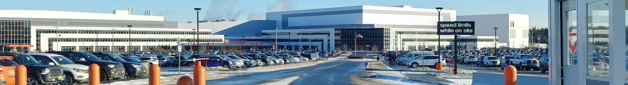
For those who haven’t noticed the anti-contaminant “bunny suit” pictures floating around Ian's Twitter page, this past weekend Ian and I took part in a tour of GlobalFoundries Fab 8 in Malta, New York. Joining a small media and analyst contingent, we were led behind-the-scenes through the cleanroom and support facilities, and had a chance to speak with select GlobalFoundries executives and managers. There wasn’t a singular purpose or focal point of the tour, and in effect it was more like GlobalFoundries impressing upon us the visceral experience of witnessing their most advanced fab in active operation. This fab, Fab 8, is where GlobalFoundries will create 7nm, with EUV rumbling into motion for them and the rest of the industry.
It is hard to overstate how rare this opportunity was, and how fortunate we were, not only in getting such unadulterated access to a semiconductor foundry’s most advanced factory, but also in walking through the actual cleanroom, where the magic is done upon the silicon wafers. There were more formal discussions later in the day, but the centerpiece was clearly the site walk, which we’ll have to describe in words (as unsurprisingly we weren’t allowed to take pictures). For such a subjective showcase, an anecdotal reflection seems more fitting to illustrate the experience; after all, even AnandTech analyst-journalists still count as journalists, reporting on what they see. Though I should note that less fluffier articles are forthcoming: a thorough news piece, AnandTech Podcast 45, and Ian’s exclusive 1-on-1 interview with GlobalFoundries CTO Gary Patton.
It was only a couple months ago since GlobalFoundries approached us with the invitation, and as Ian and I both desperately wanted to go, we both went to the fab (short for semiconductor fabrication plant). For me, a relative newcomer to AnandTech’s ranks, it felt like I was allowed a peek inside Santa Claus’ toy factory while I was still a kid and could believe in such magical things. Growing up is realizing that fabs are sophisticated sinkholes of ever-increasing capital expenditure in the eternal quest to outsmart physics, so much so that where there used to be dozens of foundries and IDMs jostling at the cutting edge, there are now just four: TSMC, Intel, Samsung, and GlobalFoundries. Of them, only TSMC and GlobalFoundries are pure-play foundries, only taking orders from fabless chip designers rather than fabbing their own designs.
Like Ian and I have discussed in the podcast, we were guided through the sub-fab and cleanroom, free to badger our escorts with all sorts of questions. I started first with the sub-fab, named so as it occupies a huge space underneath the cleanroom; 6-to-1 was the cited ratio of sub-fab to cleanroom space. Responsible for supporting the tools and sustaining the super-clean environment above it, the sub-fab is really just a labyrinth of pipes and long corridors. Looking up to the ceiling, there are pipes. Looking to the side rooms, there are boilers, giant containers, and pipes. Looking to the middle, there are rows and rows of machinery – which have pipes leading upwards. All of these carry all sorts of chemicals, liquids, and slurries necessary to carve out billions of tiny electronic flecks on a wafer. Extending outdoors were more connections, some linking to Central Utility Buildings or ultra-pure water facilities, others to tanks of oxygen, hydrogen, and liquid nitrogen, all dedicated to supporting the fab.
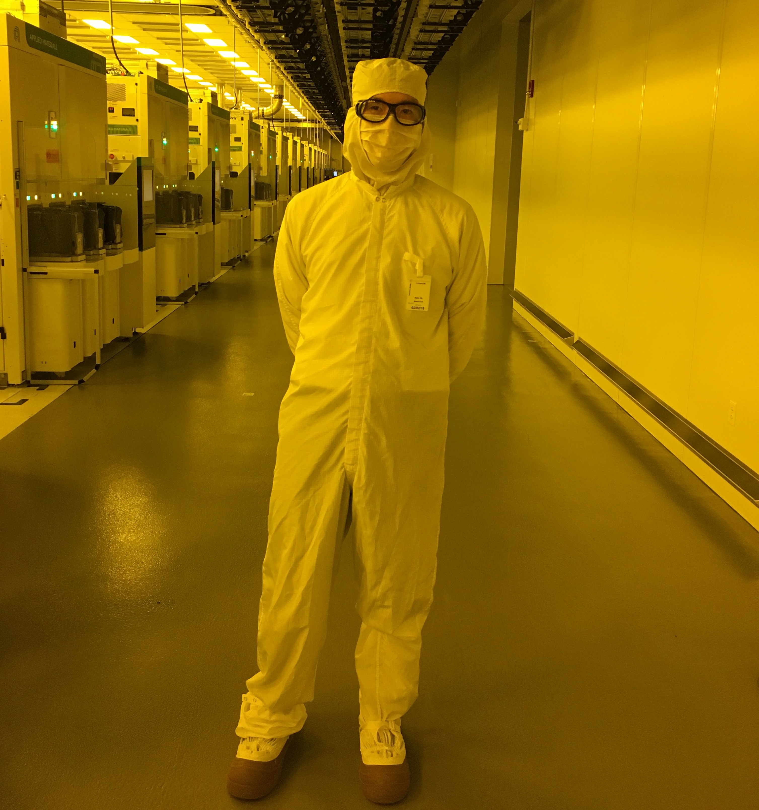
Nate Oh in a bunny suit in the Fab 8 cleanroom
To enter the cleanroom, we meticulously donned the bunny suits in proper order: glove liners, hairnet and beard cover, mask, hood, gown, boots, goggles, and finally our cleanroom ID badges. Even for the gowns, we had to put them on strategically as not to let it touch the floor. The space naturally had filters and positive air pressure to keep out as many particles as possible, but the most noticeable thing when we entered was overhead, where cart-like ‘vehicles’ zipped along while hanging from tracks on the ceiling, slowing down in traffic and speeding up on the straightaways. Transporting the amusingly named FOUPs and FOSBs, the whole system seemed distinctly like an upside-down miniature Sim City of boxes.
Meanwhile, other fab workers diligently vacuumed up the floor. Workers dealing with copper walked around with their own red-collar bunny suits, delineated that way due to possible electromigration issues. Vendors had their own grey suits, like the ASML team we saw working on the giant EUV tools, one of which was still in components of exposed pipes and wires. The familiar industrial sights of Windows XP and trackball mice poked out of the rows of boxy ASML tools, illuminated by the dim yellow lights that were still present for much of the cleanroom. All-in-all, it seemed a lot like stepping into a tiny museum-like sci-fi city.
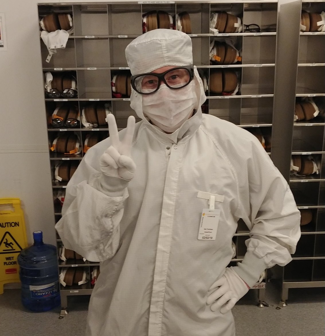
Ian Cutress in a bunny suit in the Fab 8 cleanroom gowning area
The operations engineer would tell us that this was the most automated fab in the world, where no one moves or touches the wafers at all. GlobalFoundries had built Fab 8 from the ground-up to be highly automated, and the ‘vehicles’ were the key part. For these automated machines, their locations on the tracks were monitored, and when encountering certain errors they chirped out the first bit of “Mary Had a Little Lamb,” which from a distance I honestly thought was a musical machine chorus of some kind. Each of the wafers being transported, 25 a time in one of the FOUPs, were shielded from the environment and also from light throughout the whole process. We finally got to see a wafer in one of the machines on the side, which stored defected wafers.
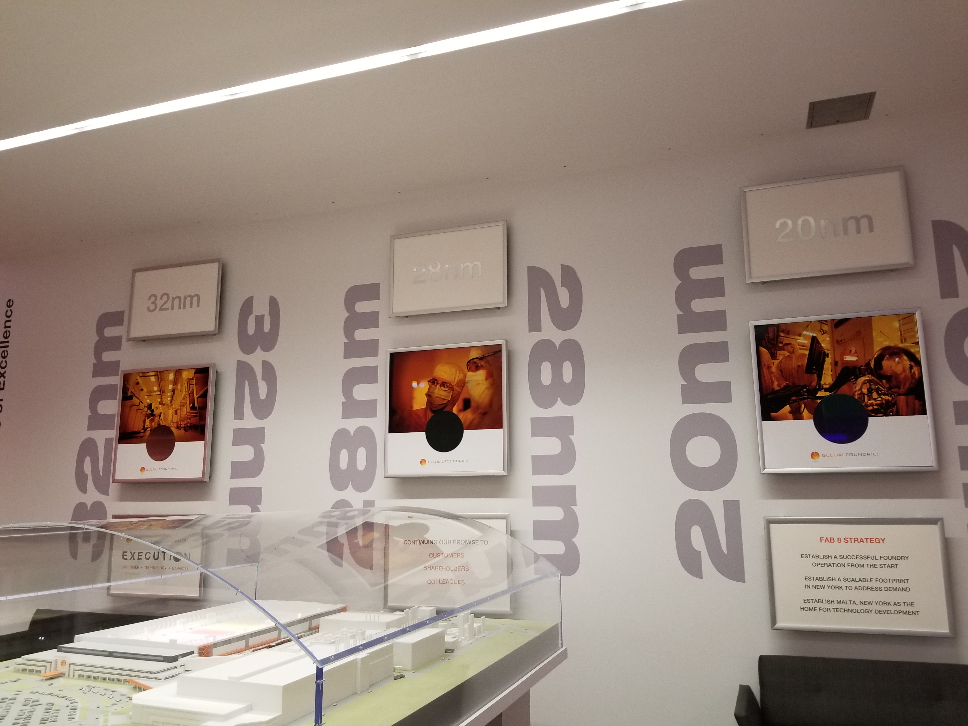
Here and there, the GlobalFoundries personnel kept referring to the analogy of an iceberg, where the cleanroom was just the most visible tip. And that theme of an outsized structure supporting one relatively small piece seems to be prevalent. I believe it was Fab 8 General Manager Tom Caulfield that called their industry a unique one because all their eggs are always in one or two process node baskets, something that GlobalFoundries brushed with in the case of 14nm. At present, they are continuing to push a dual roadmap with 12nm and 7nm FinFET on one side, and on the other, fully-depleted silicon-on-insulator (FD-SOI) for lower-cost applications. But Fab 8 is key to all of those, producing 14/12nm currently, ramping up 7nm optical, while developing EUV and researching 12nm FD-SOI. Both 7nm and FD-SOI are major junctures for them, and it will be interesting to see what they can make of it, particularly as they continue to make use of the IBM talent. And on that note, whatever the future holds for 14HP IBM process, as well as what follows on 7nm.
Even though the technology and actual manufacturing steps are known, it really is something else to see it in action, which goes double for a state-of-the-art fab. It’s strange to remember that I was actually in the cleanroom of GlobalFoundries’ Fab 8 actively churning out 14/12nm silicon, a scenario that would’ve sounded absurd a year ago because in many ways, I still think of myself as an AnandTech reader rather than an AnandTech editor. Not to mention meeting other analysts and journalists that I previously knew only as a reader of their written work.
As someone who lives very much downstate, it’s a bit funny that a little gem like this exists in upstate New York, in the sense that there are only a handful of 16/14nm fabs in the world. But I’ve definitely been lucky to visit Fab 8 like this, especially as a newcomer. I’d just like to hope that it won’t be the last fab I’ll visit.


18 Comments
View All Comments
plopke - Thursday, February 8, 2018 - link
maybe ian can wear his "bunny suit" to the next ces/convention to not catch the flue :P.deepblue08 - Thursday, February 8, 2018 - link
And also, it can be a glow in the dark suit, because you never know when the power might go out :pboeush - Thursday, February 8, 2018 - link
I won't be impressed until bunny suits actually start incorporating bunny ears. And ample cleavage... :Pmr_tawan - Sunday, February 11, 2018 - link
He would have to dance the same way as seen on very old Intel ad :)MajGenRelativity - Thursday, February 8, 2018 - link
I envy your ability to see inside a fab! It sounds like an awesome timebasroil - Thursday, February 8, 2018 - link
Having been in their less restrictive Fab 9, I can tell you visiting fabs is cool unless you actually need to visit for work, in which you'll be hating everyone (especially the applied materials process machines shown there)FreckledTrout - Thursday, February 8, 2018 - link
Thanks nice article. Would loved to have seen some photos of the automated machines. They almost sound like automated overhead mine cars.jjj - Thursday, February 8, 2018 - link
You can easily find info on those pods as it's the standard way of doing things.Here's an example https://www.entegris.com/shop/en/USD/Products/Wafe...
FreckledTrout - Thursday, February 8, 2018 - link
Thanks. You can easily find the info was a bit harder for me. I have never worked in semiconductors but have been in quite a few data centers so had no real background what I was looking for.I see they even have automated FOUP cleaner robots.
https://www.youtube.com/watch?v=oy2bBE-pG9g
woggs - Thursday, February 8, 2018 - link
"bunny suits, delineated that way due to possible electromigration issues."Not electromigration. Contamination. Copper is a silicon contaminant. Copper atoms are highly mobile within silicon and will ultimately be attracted up into the channels of transistors and ruin them. The use of copper for interconnect is to combat electromigration but the copper must be completely encased such that it never comes in contact with any of the underlying silicon.