Toshiba Launches XL-FLASH 3D SLC NAND
by Billy Tallis on August 5, 2019 9:00 AM EST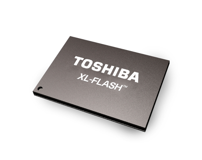
Last year at Flash Memory Summit, Toshiba announced XL-FLASH, a specialized low-latency SLC 3D NAND flash memory that is their answer to Samsung's Z-NAND (and to a lesser extent, Intel's 3D XPoint). Few details were provided at the time, but this year Toshiba is ready to give out more information, including a timeline for bringing it to market: sampling starts next month, and mass production begins next year.
The first XL-FLASH parts will use a 128Gb die, divided into 16 planes to support a much higher degree of parallelism than existing capacity-oriented 3D NAND parts. The page size will be 4kB, significantly smaller than what most 3D NAND uses, but that's not a surprise given that XL-FLASH is storing just one bit per cell rather than three or four. Toshiba's press release does not disclose the erase block size, but we expect it to be similarly smaller than what's used in high-capacity NAND designs. As for performance, Toshiba says read latency will be less than 5 microseconds, compared to about 50 µs for their 3D TLC.
The most significant difference between Toshiba's XL-FLASH and Samsung's Z-NAND may end up being the business model. Samsung's keeping Z-NAND to themselves for use in their Z-SSD products, but Toshiba's XL-FLASH will be for sale the same as their 3D TLC and QLC NAND. We have already heard from a few SSD controller vendors that they plan to support XL-FLASH in their upcoming controllers, so when XL-FLASH starts to hit the market it will probably be arriving in SSDs from several competing brands.
Flash Memory Summit kicks off tomorrow in Santa Clara, and Toshiba will be giving the first keynote presentation.


15 Comments
View All Comments
Mookid - Monday, August 5, 2019 - link
Certainly nice to have more competition in this space. Optane is great for home lab, but I’m not sure if this offers enough value for Windows gamers, or other large segments.p1esk - Monday, August 5, 2019 - link
What kind of "home lab"?Hul8 - Monday, August 5, 2019 - link
The usual kind. You should look up definitions for terms you don't understand yourself instead of being lazy.A home lab is an experimentation or learning platform you have at home, typically for stuff you would normally deploy in enterprise, like virtualization or storage. It can then double as your storage and media server.
This /r/homelab post has a few comments in the beginning that give pretty good explanations:
https://www.reddit.com/r/homelab/comments/8q1sz7/w...
mode_13h - Tuesday, August 6, 2019 - link
Eh, don't get your hackles up. I've been around the block a few times, but this is the first I've ever heard of "home lab". IMO, it's a legit question, since it's not obviously a jargon term.Samus - Wednesday, August 7, 2019 - link
I've been in IT for 20 years and have never heard the term before either. ¯\_(ツ)_/¯Dragonstongue - Monday, August 5, 2019 - link
not related but I would have expected QLC to be far less pricey than it is (for simple example, if most new release 3d/TLC on the shelf price ~$180 for 1tb then QLC should be ~$140 for the same amount (seeing as they get far far more per wafer "usable")I know business is business, however, when performance is less, takes more for the same "life span" the take for the give is cost less simply due to fact it cannot compete with even 1 gen old stuff using TLC let alone MLC drives
limitedaccess - Monday, August 5, 2019 - link
The maximum theoretical savings is 75%, or in your example $135 QLC vs $180 TLC. The problem is that savings only applies to the NAND portion. SSDs have a lot of other costs per unit and fixed costs (for the entire product line), hence by price scaling isn't linear with respect to capacity from bottom to top either.Even for the NAND portion that savings is also lower because a portion of the NAND die is not going to be cells for data storage and the added complexity means yields will be lower.
On the business side it makes sense. As with the numbers involved even a 10% savings cost wise could be millions of dollars either the manufacture or the purchase (in terms of enterprise deployments or large contracts such as laptops).
On the mainstream, consumer side the NAND price collapse over the last year really makes QLC quite meh. If prices hadn't collapsed you'd be looking at 2x the nominal savings compared to now which would be more significant. Maybe once capacity sizes on the mainstream levels go into the TB range the comparison is a 3 TB TLC drive vs a 4 TB QLC drive for the same cost they might be worth looking at again.
FunBunny2 - Monday, August 5, 2019 - link
"The problem is that savings only applies to the NAND portion."does anyone know of a forensic accounting of cost profile of SSD? in particular, what the actual proportion of SSD BoM cost is just the NAND? I suspect, but can't prove, that going from SLC to QLC means more than linear cost increase for control, both in the controller and on die.
ksec - Thursday, August 8, 2019 - link
You could do porpotion because that is not how it works. In a 128GB TLC SSD, the percentage of Controller will be much higher. Controller is a fixed cost, along with packaging, transportation etc.Controller can be anywhere from $10 to $30. Depending on supporting speed and features. You will have to DRAM as well if the SSD have it.
Another point is your QLC vs TLC scale does not take into account QLC actually have lower yield. Which means the saving are even less. Which is the reason why Companies are spending more money and time trying to stack way more layers than getting QLC polished.
ksec - Thursday, August 8, 2019 - link
You Couldn't *do