TSMC Details 3nm Process Technology: Full Node Scaling for 2H22 Volume Production
by Andrei Frumusanu on August 24, 2020 3:30 PM EST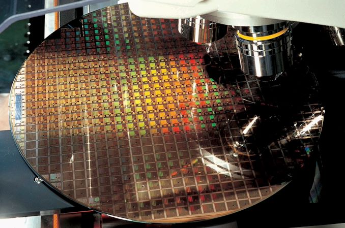
At TSMC’s annual Technology Symposium, the Taiwanese semiconductor manufacturer detailed characteristics of its future 3nm process node as well as laying out a roadmap for 5nm successors in the form of N5P and N4 process nodes.
Starting off with TSMC’s upcoming N5 process node which represents its 2nd generation deep-ultraviolet (DUV) and extreme-ultraviolet (EUV) process node after the rarely used N7+ node (Used by the Kirin 990 SoC for example). TSMC has been in mass production for several months now as we’re expecting silicon shipping to customers at this moment with consumer products shipping this year – Apple’s next-generation SoCs being the likely first candidates for the node.
TSMC details that N5 currently is progressing with defect densities one quarter ahead of N7, with the new node having better yields at the time of mass production than both their predecessor major nodes N7 and N10, with a projected defect density that’s supposed to continue to improve past the historic trends of the last two generations.
The foundry is preparing a new N5P node that’s based on the current N5 process that extends its performance and power efficiency with a 5% speed gain and a 10% power reduction.
Beyond N5P, TSMC is also introducing the N4 node that represents a further evolution from the N5 process, employing further EUV layers to reduce masks, with minimal migration work required by chip designers. We’ll be seeing N4 risk production start in 4Q21 for volume production later in 2022.
Today’s biggest news was TSMC’s disclosure on their next big leap past the N5 process node generation family, which is the 3nm N3 node. We’ve heard that TSMC had been working on defining the node back last year with progress going well.
Contrary to Samsung’s 3nm process node which makes use of GAA (Gate-all-around) transistor structures, TSMC will instead be sticking with FinFET transistors and relying on “innovative features” to enable them to achieve the full-node scaling that N3 promises to bring.
| Advertised PPA Improvements of New Process Technologies Data announced during conference calls, events, press briefings and press releases |
||||||||
| TSMC | ||||||||
| N7 vs 16FF+ |
N7 vs N10 |
N7P vs N7 |
N7+ vs N7 |
N5 vs N7 |
N5P vs N5 |
N3 vs N5 |
||
| Power | -60% | <-40% | -10% | -15% | -30% | -10% | -25-30% | |
| Performance | +30% | ? | +7% | +10% | +15% | +5% | +10-15% | |
| Logic Area Reduction % (Density) |
70% |
>37% |
- |
~17% |
0.55x -45% (1.8x) |
- |
0.58x -42% (1.7x) |
|
| Volume Manufacturing |
Q2 2019 |
Q2 2020 | 2021 | H2 2022 | ||||
Compared to it’s N5 node, N3 promises to improve performance by 10-15% at the same power levels, or reduce power by 25-30% at the same transistor speeds. Furthermore, TSMC promises a logic area density improvement of 1.7x, meaning that we’ll see a 0.58x scaling factor between N5 and N3 logic. This aggressive shrink doesn’t directly translate to all structures, as SRAM density is disclosed at only getting a 20% improvement which would mean a 0.8x scaling factor, and analog structures scaling even worse at 1.1x the density.
Modern chip designs are very SRAM-heavy with a rule-of-thumb ratio of 70/30 SRAM to logic ratio, so on a chip level the expected die shrink would only be ~26% or less.
N3 is planned to enter risk production in 2021 and enter volume production in 2H22. TSMC’s disclosed process characteristics on N3 would track closely with Samsung’s disclosures on 3GAE in terms of power and performance, but would lead more considerably in terms of density.
We’ll be posting more detailed content from TSMC’s Technology Symposium in due course, so please stay tuned for more information and updates.
Related Reading:
- TSMC: N7+ EUV Process Technology in High Volume, 6nm (N6) Coming Soon
- TSMC Announces Performance-Enhanced 7nm & 5nm Process Technologies
- TSMC: Most 7nm Clients Will Transition to 6nm
- TSMC Reveals 6 nm Process Technology: 7 nm with Higher Transistor Density
- TSMC’s 5nm EUV Making Progress: PDK, DRM, EDA Tools, 3rd Party IP Ready
- TSMC: 7nm Now Biggest Share of Revenue
- TSMC: First 7nm EUV Chips Taped Out, 5nm Risk Production in Q2 2019
- TSMC Details 5 nm Process Tech: Aggressive Scaling, But Thin Power and Performance Gains


58 Comments
View All Comments
alufan - Monday, August 24, 2020 - link
Everyone myself included poured cold water on the idea AMD may have 5nm out soon but honestly the way TSMC are going it would not surprise me if it showed up sooner rather than laterRudde - Monday, August 24, 2020 - link
With AMD at least one year, likely two years, away from releasing Zen 4 based processors, them utilising N5 for those seems like a given. On the graphics side, AMD might very well release CDNA 2 on N5 (marked 'advanced node' on their road map). Both are expected in 2022.Gondalf - Monday, August 24, 2020 - link
I don't know, N5 do not gives many advantages over N7.It is more expensive and the area scaling is delusional on cpus and GPUs. Not to mention the peak clock speed regression at the same power noticed by Qualcomm sometime ago.
The advantage of new nodes is becoming very very tiny. Architecture and higher IPC will become much more important in future and the node shrink slowly will slide in the irrelevance.
name99 - Monday, August 24, 2020 - link
"N5 do not gives many advantages over N7"And yet I expect Apple will ship cores on it that are ~30% faster than their current cores. Cores that are good for phones, watches, and desktops. And that have an accompanying GPU perhaps ~40% faster than the current GPU.
We heard this same story about 7nm being no big deal compared to 10nm.
If your CPU design flow is based around the idea that future processes get more and more dense, you can do pretty well. On the other hand, if your CPU design flow is based around the idea that you can keep cranking up the GHz...
More interesting is the way SRAM doesn't shrink much. TSMC being what they are, they won't tell us until this is ready, but one path forward is 3D. It's just a matter of time before someone ships parts like that in mass quantities. (Sure, Intel will be first to announce, like always... But I'm more interested in who's first to actually ship in bulk.)
The most trivial version of this is an SRAM chip stacked on a logic chip, but more interesting is 3D bulk fabrication, either double decker (n/p stacking) transistors, or run the wafer through the line twice.
Tomatotech - Monday, August 24, 2020 - link
How hot does SDRAM run vs logic?If it runs cool, then yeah stack it. If it runs hot because of high use, then stacking it will be problematic.
We might end up with areas of fast, hot, well-cooled, single layer SRAM and areas of cool stacked slower SDRAM.
Tomatotech - Monday, August 24, 2020 - link
Edit SRAM not bloody autocorrect SDRAMnandnandnand - Monday, August 24, 2020 - link
There was the Samsung 3D TSV SRAM story recently. I don't think they gave any details about cooling, and it might be mobile-focused.Santoval - Sunday, January 31, 2021 - link
The main hurdle to 3D stacking has always been how to keep the stacks cool. Intel's Lakefield has a mere 7W of TDP but it cannot operate its "big" Sunny Cove core continuously, only in short bursts for "fast responsiveness" (look up its review here if you have not read it). It is firmware prohibited to run single threaded code for more than a few moments at a time due to excessive heat generation.This is how the TDP was limited to 7W, among other power optimizations. And that's despite "kneecapping" the Sunny Cove core to have "feature parity" with the small cores. Both AVX-512 *and* AVX-256 were disabled because the small Tremont cores lack them (this is why AVX-256 support is to be added to Gracemont; so that the Golden Cove cores of Alder Lake will have only AVX-512 disabled ... right when AMD adds such support to Zen 4).
Imagine if 7W of TDP was so much a thermal trouble how infernally hot a 45W TDP 3D stacked chip would run if it lacked active cooling between the dies (microfluidic cooling is unfortunately still lab confined). It is literally impossible to do this and completely beyond the bounds of reality for even higher TDP CPUs. Maybe it's possible up to 25W of TDP, but these 25W parts would require equivalent cooling to what's normally required for 65W non stacked parts (or higher) to compensate. 15W should be less of a problem, but preferably the TDP should be limited to 10 - 12W. No more.
brantron - Monday, August 24, 2020 - link
Intel already showed plans for multi-chip packages using several variations of 10nm. That could become the norm, with a dedicated manufacturing process for particular circuits.If a new node overall is cost prohibitive, it would likely still be used right away for new iPhones. Apple could just do what everyone else already does, with different SoCs for the regular vs. Pro models.
Costs will go down over time, so there would just be a delay before widespread adoption.
Rudde - Tuesday, August 25, 2020 - link
+15% performance or -30% power is not to be disregarded. It's not as great as the halved power between Global Foundries 12nm and TSMC N7. That halved power consumption allowed AMD to pack 8 cores in a low power (15W) processor and 16 cores at 3.5GHz base clock in a 105W processor. Neither would have been possible at 12nm.N5 will further increase performance while keeping power consumption down. It will not necessarily manifest in higher clocks, but in increased instructions per clock (IPC) and core counts.