TSMC to Spend $100B on Fabs and R&D Over Next Three Years: 2nm, Arizona Fab & More
by Anton Shilov on April 2, 2021 10:00 AM EST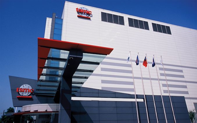
TSMC this week has announced plans to spend $100 billion on new production facilities as well as R&D over the next three years. The world's largest contract maker of chips says that its fabs are currently working at full load, so to meet demand for its services going forward it will need (much) more capacity. Among TSMC's facilities to go online in the next three to four years are the company's fab in Arizona as well as its first 2nm-capable fab in Taiwan.
"TSMC is entering a period of higher growth as the multiyear megatrends of 5G and HPC are expected to fuel strong demand for our semiconductor technologies in the next several years," a statement by TSMC with the Taiwan Stock Exchange reads. "In addition, the COVID-19 pandemic also accelerates digitalization in every aspect. In order to keep up with demand, TSMC expects to invest $100 billion over the next three years to increase capacity to support the manufacturing and R&D of advanced semiconductor technologies. TSMC is working closely with our customers to address their needs in a sustainable manner."
$100 Billion to Be Spent on Fabs
TSMC's capital expenditures (CapEx) budget last year was $17.2 billion, whereas its R&D budget was $3.72 billion, or approximately 8.2% of its revenue. This year the company intends to increase its CapEx to somewhere in the range of $25 to $28 billion, which would make for a 45% to 62% year-over-year increase in that spending. The company's R&D spending will also rise as its revenue is expected to grow. In total, TSMC plans to invest around $30 billion or more on CapEx and R&D this year. Taken altogether, if the company intends to spend around $100 billion from 2021 through 2023, its expenditures in the next two years will be roughly flat with 2021, something that should please its investors.
TSMC has a number of important fab projects ahead of it.
- First up, the company needs to build and equip its N5-capable fab in Arizona. The facility will cost around $12 billion, will have a capacity of 20,000 wafer starts per month (WSPM), and will come online in 2024. A recent rumor indicates that TSMC might actually increase capacity of the facility and/or equip it for a more advanced fabrication process, which will increase its cost, but TSMC has never confirmed this information.
- Secondly, TSMC will need to equip its N3-capable fab in Tainan, Taiwan, which is projected to start volume production in the second half of 2022.
- TSMC's third capital-expensive project is the company's N2 (2nm) qualified GigaFab in Hsinchu, Taiwan. Furthermore, TSMC is mulling to build another N2-capable fab in Baoshan, Taiwan. Meanwhile, TSMC still has to complete development of its GAAFET-based N2 node.
- Last but not least, TSMC is set to build two more advanced packaging facilities in Taiwan. The company already has four of such facilities, but it believes that demand for chip stacking and advanced packaging will rise in the future and it will need more capacities. Chip packaging factories are not as expensive as semiconductor production facilities, but they still cost quite a lot.
Recently TSMC wrote a letter to its customers where it explained that its fabs have been fully utilized for about a year now and it still cannot meet rising demand for chips. To that end, the company would have to 'suspend wafer price reductions for a year from the start of 2022,' according to a Bloomberg report.
Competition Intensifying
Right now, TSMC is the world's largest contract maker of chips with no rivals that can match its total production capacity. A some of TSMC's rivals, including GlobalFoundries and UMC, have pulled the plug on development of their leading-edge fabrication processes, so the number of companies that can offer leading-edge nodes has decreased. Yet paradoxically, the competition is also escalating in other respects.
Samsung Semiconductor, which has foundry, DRAM, storage, SoC, and a number of other operations, has been increasing its CapEx investments in the recent years. The company spent $93.2 billion on chip production from 2017 to 2020 and is on track spend another ~$28 billion in 2021, according to IC Insights. Samsung Foundry is still several times smaller than TSMC in terms of sales and capacity, but the gap is closing.
In addition to Samsung Foundry, Intel recently introduced its integrated device manufacturer 2.0 (IDM 2.0) plan that includes offering advanced foundry services and essentially compete against TSMC (while also using its services when needed). Intel has already announced plans to invest $20 billion in two new fabs in Arizona and said it would invest more in expansion of chip production in other parts of the USA as well as in Europe and other parts of the world.
To stay ahead of existing and emerging rivals, TSMC needs to keep investing in R&D and expand its production capacities, so a $100 billion investment plan will be instrumental for these purposes.


44 Comments
View All Comments
WaltC - Friday, April 2, 2021 - link
If the AZ FAB is still on, that's great! I thought I had read something about TSMC deciding not to expand its FABs in the EU and elsewhere...so evidently the TSMC AZ FAB is still on the list to be completed!DanNeely - Friday, April 2, 2021 - link
The AZ fab has a more or less guaranteed set of customers in the form of the US Govt/DoD who want a more modern domestic fab to contract sensitive parts to than what GF can provide. A few years ago, that probably would've been Intel; but after their 10nm faceplant the pentagon probably isn't willing to gamble on them actually delivering on their announced foundry services.Smell This - Friday, April 2, 2021 - link
The gub'mint does not do bleeding edge ___ they most likely are at 32 / 28nm node
Spunjji - Friday, April 2, 2021 - link
Depends on what they're doing with the chips - and by 2024 (and beyond) I suspect they'd find a use for 5nm manufacturing *somewhere*.Molor1880 - Friday, April 2, 2021 - link
The DoD is buying Frontier (OLCF-5) for the DoE. That's 7nm EPIC chips.DanNeely - Friday, April 2, 2021 - link
For that stuff they can keep using GloFo's old legacy process fabs. They do have some stuff that would benefit from much higher transistor densities that they really don't want to send overseas. That's why they've been pushing to get someone to build a modern contract fab inside the US.flgt - Friday, April 2, 2021 - link
I imagine someone finally realized all the commercial chips that were going in their systems from companies like Xilinx. The question is can the government make AMD/Xilinx uses a commercially non-competitive fab in the US. If they were smart they would take some of that $700B defense budget and make it worth everyone’s effort.Kamen Rider Blade - Friday, April 2, 2021 - link
But by the time the AZ fab is done, 5nm is going to be a old processSamus - Sunday, April 4, 2021 - link
"Old process" or not, when you consider how many products are still produced now in the 20-30nm class (chipsets, modems, ASICs, FPGAs, etc) there will be 5nm demand for over a decade as these products slowly transition to smaller processes - but they wont until those processes are mature, inexpensive, and actually available (current 5-7nm demand is above 100% and will be for at least another year)Zoolook - Monday, April 5, 2021 - link
Considering that the military wants their chips hardened, current 5 nm isn't really for them.