NVIDIA's GeForce GTX 465: Cheaper Isn’t Always Better
by Ryan Smith on May 31, 2010 3:26 AM ESTIn recent years it’s become customary to have 3-4 high-end cards on the market at the same time using the same GPU. For the GTX 200 series we had the GTX 260, GTX 275, and GTX 285, while for the Radeon HD 5000 series we have the 5830, 5850, and 5870. With the launch of NVIDIA’s GTX 400 series last month NVIDIA filled in the first 2 spots in their lineup with the GTX 480 and GTX 470, with obvious room to grow out the family in the future.
Above the GTX 480 is of course the “full” GF100 with all of its functional units enabled, and which is still missing in action on both the consumer and HPC markets. However there’s also room for a card below the $350 GTX 470, particularly with AMD being the sole inhabitant of the “bargain” high-end $300 point. NVIDIA is to the point in the Fermi rollout where they want a piece of that market, and they have a stash of further-binned so-so GF100 chips they want to fill it with. This brings us to today, and the launch of the GeForce GTX 465.
| GTX 480 | GTX 470 | GTX 465 | GTX 285 | |
| Stream Processors | 480 | 448 | 352 | 240 |
| Texture Address / Filtering | 60/60 | 56/56 | 44/44 | 80 / 80 |
| ROPs | 48 | 40 | 32 | 32 |
| Core Clock | 700MHz | 607MHz | 607MHz | 648MHz |
| Shader Clock | 1401MHz | 1215MHz | 1215MHz | 1476MHz |
| Memory Clock | 924MHz (3696MHz data rate) GDDR5 | 837MHz (3348MHz data rate) GDDR5 | 802MHz (3208MHz data rate) GDDR5 | 1242MHz (2484MHz data rate) GDDR3 |
| Memory Bus Width | 384-bit | 320-bit | 256-bit | 512-bit |
| Frame Buffer | 1.5GB | 1.25GB | 1GB | 1GB |
| Transistor Count | 3B | 3B | 3B | 1.4B |
| Manufacturing Process | TSMC 40nm | TSMC 40nm | TSMC 40nm | TSMC 55nm |
| Price Point | $499 | $349 | $279 | N/A |
In a nutshell, if you take a GTX 470 and disable some additional functional units, additional memory controllers, and additional ROPs, while turning down the memory speed any further, you get the GTX 465. NVIDIA has shut off another 3 Streaming Multiprocessors (SMs) from GF100, leaving the GTX 465 with 11 of them, giving it a total of 352 CUDA Cores/SPs, and 44 texture units. Meanwhile the ROPs have been cut down to 32 ROPs, and another memory controller disabled, making for a 256-bit memory bus attached to 1GB of 802MHz (3208MHz effective) GDDR5. All told the GTX 465 has around 78% of the texture/shader power of the GTX 470, 80% the ROP power, 76% of the memory bandwidth of the GTX 470, and 80% of the memory capacity. The loss of 256MB of RAM will be particularly interesting, as it means NVIDIA has surrendered its memory capacity advantage over AMD’s reference cards – both are even at 1GB.
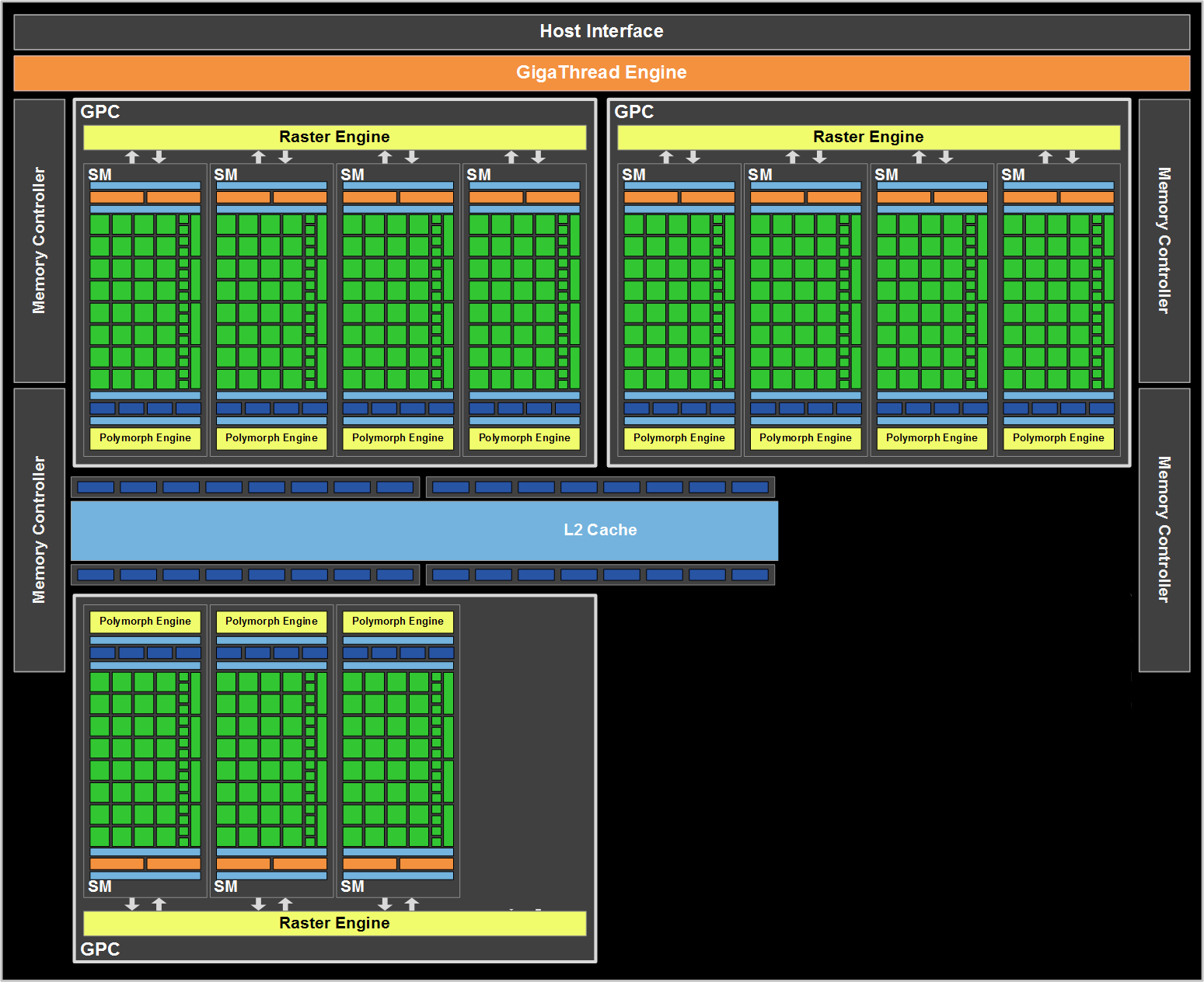
With all of that in mind, compared to the GTX 470 the GTX 465 may be the more interesting card. While NVIDIA simply disabled some additional functional units compared to the GTX 480 to get the GTX 470, disabling even more functional units required a different strategy. Rather than disabling additional units from each of the GF100 GPU’s 4 Graphics Processing Clusters (GPCs), NVIDIA outright disabled one of the GPCs. This is the first time we’ve seen them disable a GPC on a GF100 card, making it an interesting first for Fermi. By disabling a GPC, not only does NVIDIA surrender CUDA cores, texture units, and polymorph engines, but they also surrender one of the 4 raster engines. As a result the GTX 465 takes a straight 25% hit in rasterization abilities compared to GTX 470, slightly greater than the loss for any other part of the GTX 465.

Top: GTX 465. Bottom: GTX 470
Along with similar clockspeeds as the GTX 470, the GTX 465 also shares the GTX 470’s design. It’s the same PCB and cooler – only the GPU has changed, with NVIDIA’s partners laying down one of NVIDIA’s GTX 465-binned GF100 GPUs.
With the disabling of additional functional units, the TDP has come down compared to the GTX 470. NVIDIA pegs the GTX 465 at 200W TDP, 15W below the GTX 470’s official TDP. We were not given the idle power consumption; however we’ll see quickly that it hasn’t improved when looking at our own power consumption numbers.
As we stated earlier, this is NVIDIA’s shot at the sub-$300 market, which is currently dominated by the Radeon HD 5850 at $289 and up, and the Radeon HD 5830 at $225 and up. Like the GTX 470, NVIDIA has built a product to slot in between AMD’s cards in terms of performance rather than taking AMD head-on, and the pricing reflects this. The MSRP of the GTX 465 is $279 accordingly, maintaining AMD and NVIDIA’s more-or-less neat division of the high-end market and putting the performance “sweet spot” for the GTX 465's performance at roughly 93% of the 5850.
Meanwhile this is the closest the two have come on pricing in quite some time, as a $279 MSRP puts the GTX 465 within $10 of the cheapest Radeon HD 5850. The pricing on the GTX 465 may change in the next month as NVIDIA’s North American partners are currently packing in Just Cause 2 with the card (a last-minute deal as we understand it), so there may be some flexibility on pricing once that promotion ends and NVIDIA’s partners no longer have to chip in for the game.
Finally, this is a hard launch, a very hard launch. In fact the cards started showing up on etailers 2 days before our NDA expired. After the farce that was the GTX 480/470 launch, it’s fantastic to see a proper hard launch. As far as we can tell you won’t have any problem finding a GTX 465 – thanks in large part to what looks to be quite the stockpile of GF100 GPUs that only meet GTX 465 specifications.


71 Comments
View All Comments
poohbear - Monday, May 31, 2010 - link
Why's the 5770 10fps slower than the 4870? is that a mistake? they perform on par especially w/ the recent driver updates for the 5770.poohbear - Monday, May 31, 2010 - link
in mass effect 2.:p hate the no edit feature!Ryan Smith - Monday, May 31, 2010 - link
There aren't any typos; those are the results we got for those cards on the 10.3a drivers.temps - Monday, May 31, 2010 - link
I can vouch for that. When my 1gb 4870 died, it was replaced with a 5770. In ME2, I saw a 10-15fps drop across the board with the same settings.. that didn't do it for me, so I ended up stepping up to a 5850.BoFox - Tuesday, June 1, 2010 - link
Didn't you know that the 5770 is generally slower than 4870? The 4870 has far, far greater memory bandwidth despite a 100MHz lower core clock.tno - Monday, May 31, 2010 - link
I think a repost to the feed is appropriate when someone goes through this again and polishes it up. I couldn't finish the second paragraph it was so full or mistakes. Really guys there is no shame in hiring a copy editor.softdrinkviking - Tuesday, June 1, 2010 - link
i don't care about typos in this kind of article.aside from problems with the numbers, i think everyone knows what is meant.
i feel like it's expected that tech blog sites are littered with typos.
actually, i'd like to hear about this from ryan smith or somebody here.
do you guys want us to post typo corrections in the comments?
i don't care, but what does anandtech want?
taltamir - Monday, May 31, 2010 - link
According to the graph, the GTX465 gets 89 C not 91 C.
taltamir - Monday, May 31, 2010 - link
nevermind, I see now that there are two graphs, one for furmark and one for crysis.multivac - Monday, May 31, 2010 - link
NVIDIA filled in the first 2 spots in their lineup with the GTX 480 and GTX 480, with obvious room to grow out the family in the future.end of the first paragraph.
still reading but im sure its a great article
cheers!