Semiconductors

This week Samsung Electronics and Synopsys announced that Samsung has taped out its first mobile system-on-chip on Samsung Foundry's 3nm gate-all-around (GAA) process technology. The announcement, coming from electronic design automation Synopsys, further notes that Samsung used the Synopsys.ai EDA suite to place-n-route the layout and verify design of the SoC, which in turn enabled higher performance. Samsung's unnamed high-performance mobile SoC relies on 'flagship' general-purpose CPU and GPU architectures as well as various IP blocks from Synopsys. SoC designers used Synopsys.ai EDA software, including the Synopsys DSO.ai to fine-tune design and maximize yields as well as Synopsys Fusion Compiler RTL-to-GDSII solution to achieve higher performance, lower power, and optimize area (PPA). And while the news that Samsung has developed a high-performance SoC using the Synopsys.ai...

GlobalFoundries Sells Off Photomask Assets to Toppan
Following its decision to focus on specialized process technologies last August, GlobalFoundries has been consolidating its assets as well as selling off businesses and facilities that are not essential...
20 by Anton Shilov on 8/15/2019
Samsung’s Aggressive EUV Plans: 6nm Production in H2, 5nm & 4nm On Track
Samsung Foundry formally started to produce chips using its 7LPP (7 nm low power plus) fabrication process last October and has not slowdown development of its manufacturing technologies since...
42 by Anton Shilov on 7/31/2019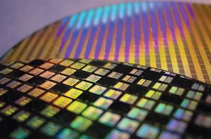
TSMC Announces Performance-Enhanced 7nm & 5nm Process Technologies
TSMC has quietly introduced a performance-enhanced version of its 7 nm DUV (N7) and 5 nm EUV (N5) manufacturing process. The company’s N7P and N5P technologies are designed for...
36 by Anton Shilov on 7/30/2019
LG Display & SK Hynix Looking to Diversify Industrial Suppliers as Row with Japan Intensifies
South Korean electronics companies reaffirmed this week that production of computer memory and displays could be disrupted because of ongoing trade dispute between the country and Japan. Both SK...
8 by Anton Shilov on 7/26/2019
TSMC: 3nm EUV Development Progress Going Well, Early Customers Engaged
Development of new fabrication technologies never stops at leading-edge companies such as TSMC. Therefore, it is not surprising to hear the annoucement that development of TSMC’s 3nm node is...
76 by Anton Shilov on 7/23/2019
Samsung’s 5nm EUV Technology Gets Closer: Tools by Cadence & Synopsys Certified
Samsung Foundry has certified full flow tools from Cadence and Synopsys for its 5LPE (5 nm low-power early) process technology that uses extreme ultraviolet lithography (EUV). Full flow design...
13 by Anton Shilov on 7/8/2019
Synopsys to Accelerate Samsung’s 7nm Ramp with Yield Explorer Platform
Synopsys has announced an acceleration of development on its yield learning platform designed to speed up ramp up of chips made using Samsung Foundry’s 7LPP (7 nm low power...
16 by Anton Shilov on 7/4/2019Marvell to Acquire Avera Semiconductor from GlobalFoundries
Marvell on Monday announced that it had entered into agreement to buy Avera Semiconductor from GlobalFoundries. The acquisition will bring additional chip design capabilities to Marvell and will enable...
8 by Anton Shilov on 5/20/2019_carousel.jpg)
Samsung Announces 3nm GAA MBCFET PDK, Version 0.1
So what comes after 7nm, after 6nm, after 5nm, and after 4nm? That's right: 3nm! At Samsung's Foundry Forum event today, Samsung has announced that the first alpha version...
32 by Dr. Ian Cutress on 5/14/2019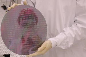
Intel Process Technology Update: 10nm Server Products in 1H 2020, Accelerated 7nm in 2021
Intel provided an update regarding its upcoming fabrication technologies at its 2019 Investor Meeting. The company is on track to produce server-class products using its 10 nm manufacturing technology...
74 by Anton Shilov on 5/8/2019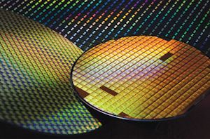
TSMC: Most 7nm Clients Will Transition to 6nm
In this week's quarterly earnings conference call, TSMC’s revealed that the company expects most of its 7nm "N7" process customers to eventually transition to its forthcoming 6nm "N6" manufacturing...
39 by Anton Shilov on 5/1/2019
Samsung to Invest $115 Billion in Foundry & Chip Businesses by 2030
Being among the largest contract makers of semiconductors and among leading developers of chips for various applications, Samsung Electronics wants to become the world’s leader in these industries. To...
27 by Anton Shilov on 4/24/2019
GlobalFoundries to Sell 300mm New York Fab to ON Semiconductor
GlobalFoundries and ON Semiconductor on Monday signed a definitive agreement for the latter to buy GlobalFoundries’ 300-mm fab in East Fishkill, New York. In addition to the production facility...
25 by Anton Shilov on 4/22/2019
TSMC: No Plans to Buy Rivals at The Moment
Although TSMC expects demand for chips to increase going forward and despite an ongoing trend towards consolidation on the foundry market, the company has commented that it currently has...
4 by Anton Shilov on 4/22/2019
Samsung Completes Development of 5nm EUV Process Technology
Samsung Foundry this week announced that it has completed development of its first-generation 5 nm fabrication process (previously dubbed 5LPE). The manufacturing technology uses extreme ultraviolet lithography (EUVL) and...
21 by Anton Shilov on 4/17/2019
TSMC Reveals 6 nm Process Technology: 7 nm with Higher Transistor Density
TSMC this week unveiled its new 6 nm (CLN6FF, N6) manufacturing technology, which is set to deliver a considerably higher transistor density when compared to the company's 7 nm...
23 by Anton Shilov on 4/17/2019
TSMC’s 5nm EUV Making Progress: PDK, DRM, EDA Tools, 3rd Party IP Ready
TSMC this week has said that it has completed development of tools required for design of SoCs that are made using its 5 nm (CLN5FF, N5) fabrication technology. The...
33 by Anton Shilov on 4/5/2019
GlobalFoundries and Synopsys Develop Automotive-Grade IP for 22FDX Process Tech
GloalFoundries and Synopsys announced this week that they have jointly developed a portfolio of automotive-gade IP solutions for GF’s 22FDX process technology. The various IP blocks are designed for...
4 by Anton Shilov on 2/22/2019
TSMC’s Fab 14B Photoresist Material Incident: $550 Million in Lost Revenue
TSMC on Friday revealed more details regarding an incident with a photoresist material at its Fab 14B earlier this year. The contaminated chemical damaged wafers on TSMC’s 12 nm...
29 by Anton Shilov on 2/20/2019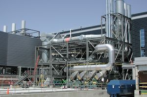
Intel Submits Ireland Fab Expansion Plan: $8 Billion Price Tag, With a 4 Year Lead Time
Intel has submitted a proposal to Irish authorities for the expansion of its manufacturing site near Leixlip. According to the plans, Intel is exploring the construction of a brand-new...
27 by Anton Shilov on 2/13/2019


